AD8344
Rev. 0 | Page 15 of 20
The high input impedance of the AD8351 allows for a shunt
differential termination to provide the desired 200 Ω load to the
AD8344 IF output port.
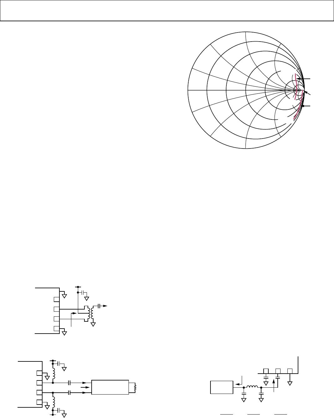
It is necessary to bias the open collector outputs using one of
the schemes presented in Figure 39 and Figure 40. Figure 39
illustrates the application of a center-tapped impedance trans-
former. The turns ratio of the transformer should be selected to
provide the desired impedance transformation. In the case of a
50 Ω load impedance, a 4-to-1 impedance ratio transformer
should be used to transform the 50 Ω load into a 200 Ω
differential load at the IF output pins. Figure 40 illustrates a
differential IF interface where pull-up choke inductors are used
to bias the open-collector outputs. The shunting impedance of
the choke inductors used to couple dc current into the mixer
core should be large enough at the IF frequency of operation as
to not load down the output current before reaching the
intended load. Additionally, the dc current handling capability
of the selected choke inductors needs to be at least 45 mA. The
self resonant frequency of the selected choke should be higher
than the intended IF frequency. A variety of suitable choke
inductors are commercially available from manufacturers such
as Murata and Coilcraft. An impedance transforming network
may be required to transform the final load impedance to 200 Ω
at the IF outputs. There are several good reference books that
explain general impedance matching procedures, including:
Chris Bowick, RF Circuit Design, Newnes, Reprint Edition,
1997.
David M. Pozar, Microwave Engineering, Wiley Text Books,
Second Edition, 1997.
Guillermo Gonzalez, Microwave Transistor Amplifiers: Analy-
sis and Design, Prentice Hall, Second Edition, 1996.
04826-0-042
COMM
8
IFOP
7
IFOM
6
COMM
5
AD8344
Z
L
=
2
0
0
I
F
O
U
T
Z
O
=
5
0
+
V
S
4:1
Figure 39. Biasing the IF Port Open Collector Outputs
Using a Center-Tapped Impedance Transformer
04826-0-043
COMM
8
IFOP
7
IFOM
6
COMM
5
AD8344
R
F
C
+
V
S
R
F
C
Z
L
=
2
0
0
I
F
O
U
T
+
I
F
O
U
T
+
V
S
Z
L
IMPEDANCE
TRANSFORMING
NETWORK
Figure 40. Biasing the IF Port Open Collector Outputs
Using Pull-Up Choke Inductors
04826-0-044
0180
30
330
50MHz
50MHz
500MHz
500MHz
60
90
270
300
120
240
150
210
REAL
CHOKES
IDEAL
CHOKES
Figure 41. IF Port Loading Effects due to Finite-Q Pull-Up Inductors
(Murata BLM18HD601SN1D Chokes)
LO CONSIDERATIONS
The LO signal needs to have adequate phase noise characteris-
tics and reasonable low second harmonic content to prevent
degradation of the noise figure performance of the AD8344. A
LO plagued with poor phase noise can result in reciprocal
mixing, a mechanism that causes spectral spreading of the
downconverted signal, limiting the sensitivity of the mixer at
frequencies close-in to any large input signals. The internal LO
buffer provides enough gain to hard limit the input LO and
provide fast switching of the mixer core. Odd harmonic content
present on the LO drive signal should not impact mixer
performance; however, even-order harmonics cause the mixer
core to commutate in an unbalanced manner, potentially
degrading noise performance. Simple lumped element low-pass
filtering can be applied to help reject the harmonic content of a
given local oscillator, as illustrated in Figure 42. The filter
depicted is a common 3-pole Chebyshev, designed to maintain a
1-to-1 source-to-load impedance ratio with no more than
0.5 dB of ripple in the pass band. Other filter structures can be
effective as long as the second harmonic of the LO is filtered to
negligible levels, e.g., ~30 dB below the fundamental. The meas-
ured frequency response of the Chebyshev filter for a 1200 MHz
−3 dB cutoff frequency is presented in Figure 43.
04826-0-045
AD8344
LOIN
3
COMM
4
LOCM
2
R
L
FOR R
S
= R
L
f
C
- FILTER CUTOFF FREQUENCY
R
S
C1 C3
LO
SOURCE
L2
C1 =
1.864
2
πf
c
R
L
C3 =
1.834
2
πf
c
R
L
L2 =
1.28R
L
2
πf
c
Figure 42. Using a Low-Pass Filter to Reduce LO Second Harmonic
AD8344
Rev. 0 | Page 16 of 20
0
–50
–45
–40
–35
–30
–25
–20
–15
–10
–5
0.1 1 10
04826-0-046
FREQUENCY (GHz)
RESPONSE (dB)
IDEAL LPF
REAL LPF
4.7pF 4.7pF
6.8nH
Figure 43. Measured and Ideal LO Filter Frequency Response
BIAS RESISTOR SELECTION
An external bias resistor is used to set the dc current in the
mixer core. This provides the ability to reduce power consump-
tion at the expense of decreased dynamic range. Figure 44
shows the spurious-free dynamic range (SFDR) of the mixer for
a 1 Hz noise bandwidth versus the R
BIAS
resistor value. SFDR
was calculated using NF and IIP3 data collected at 900 MHz.
By definition,
()
)(10log
3
2
BkTNFIIP3SFDR =
where IIP3 is the input third-order intercept in dBm. NF is the
noise figure in dB. kT is the thermal noise power density and is
−173.86 dBm/Hz at 298°K. B is the noise bandwidth in Hz.
In order to calculate the anticipated SFDR for a given applica-
tion, it is necessary to factor in the actual noise bandwidth. For
instance, if the IF noise bandwidth was 5 MHz, the anticipated
SFDR using a 2.43 kΩ R
BIAS
would be 6.66 log10 (5 MHz) less
than the 1 Hz data in Figure 44 or ~80 dBc. Using a 2.43 kΩ bias
resistor will set the quiescent power dissipation to ~415 mW for
a 5 V supply. If the R
BIAS
resistor value was raised to 3.9 kΩ, the
SFDR for the same 5 MHz bandwidth would be reduced to
~77.5 dBc and the power dissipation would be reduced to
~335 mW. In low power portable applications it may be advanta-
geous to reduce power consumption by using a larger value of R
BIAS
,
assuming reduced dynamic range performance is acceptable.
125
120
85
81
77
73
69
65
121
122
123
124
2.4 2.6 2.8 3.0 3.2 3.4 3.6 3.8 4.0
04826-0-047
R
BIAS
(k)
SFDR (dBc)
SUPPLY CURRENT (mA)
AD8344
COMM
9
EXRB
10
PWDN
11
VPDC
12
+V
S
R
BIAS
Figure 44. Impact of R
BIAS
Resistor Selection vs. Spurious-Free
Dynamic Range and Power Consumption,
F
RF
= 890 MHz and F
LO
= 1090 MHz
CONVERSION GAIN AND IF LOADING
The AD8344 is optimized for driving a 200 Ω differential load.
Although the device is capable of driving a wide variety of
loads, in order to maintain optimum distortion and noise
performance, it is advised that the presented load at the IF
outputs is reasonably close to 200 Ω. Figure 45 illustrates the
effect of IF loading on conversion gain. The mixer outputs
behave like Norton equivalent sources, where the conversion
gain is the effective transconductance of the mixer multiplied
by the loading impedance. The linear differential voltage
conversion gain of the mixer can be modeled as
RF
m
m
LOAD
fgj
g
RAv
×××+
××=
37.701
0.46
where R
LOAD
is the differential loading impedance. g
m
is the
mixer transconductance and is equal to 4070/R
BIAS
. f
RF
is the
frequency of the signal applied to the RF port in GHz.
Large impedance loads cause the conversion gain to increase,
resulting in a decrease in input linearity and allowable signal
swing. In order to maintain positive conversion gain and pre-
serve spurious-free dynamic range performance, the differential
load presented at the IF port should remain within a range of
~100 Ω to 250 Ω.
AD8344
Rev. 0 | Page 17 of 20
25
–5
0
5
10
15
20
10 100 1000
04826-0-048
IF LOADING (
)
20LOG–CONVERSION GAIN (dB)
MEASURED
MODELED
15
0
15
12
9
6
3
0
3
6
9
12
10 15 20 25 30 35 40 45 50
04826-0-049
IF FREQUENCY (MHz)
CONVERSION GAIN (dB)
INPUT IP3 AND P1dB (dBm)
Figure 45. Conversion Gain vs. IF Loading Figure 46. Conversion Gain, Input IP3, and P1dB vs.
IF Frequency, F
RF
= 450 MHz
LOW IF FREQUENCY OPERATION
8
7
2
28.0
24.5
21.0
17.5
14.0
10.5
7.0
3
4
5
6
10 15 20 25 30 35 40 45 50
04826-0-050
IF FREQUENCY (MHz)
CONVERSION GAIN (dB)
INPUT IP3 AND P1dB (dBm)
The AD8344 may be used down to arbitrarily low IF frequen-
cies. The conversion gain, noise, and linearity characteristics
remain quite flat as IF frequency is reduced, as indicated in
Figure 46 and Figure 47. Larger value pull-up inductors need to
be used at the lower IF frequencies. A 1 µH choke inductor
would present a common-mode loading impedance of 63 Ω at
an IF frequency of 10 MHz, severely loading down the mixer
outputs, reducing conversion gain, and sacrificing output power.
At low IF frequencies, choke inductors of several hundred µH
should be used for biasing the IF outputs.
Figure 47. Conversion Gain, Input IP3, and P1dB vs.
IF Frequency, F
RF
= 890 MHz

AD8344ACPZ-REEL7

Mfr. #:
Manufacturer:
Analog Devices Inc.
Description:
RF Mixer IC 400MHz - 1.2GHz Active Receive
Lifecycle:
New from this manufacturer.
Delivery:
DHL FedEx Ups TNT EMS
Payment:
T/T Paypal Visa MoneyGram Western Union

Products related to this Datasheet