April 2005 23 M9999-041405
KS8721CL Micrel, Inc.
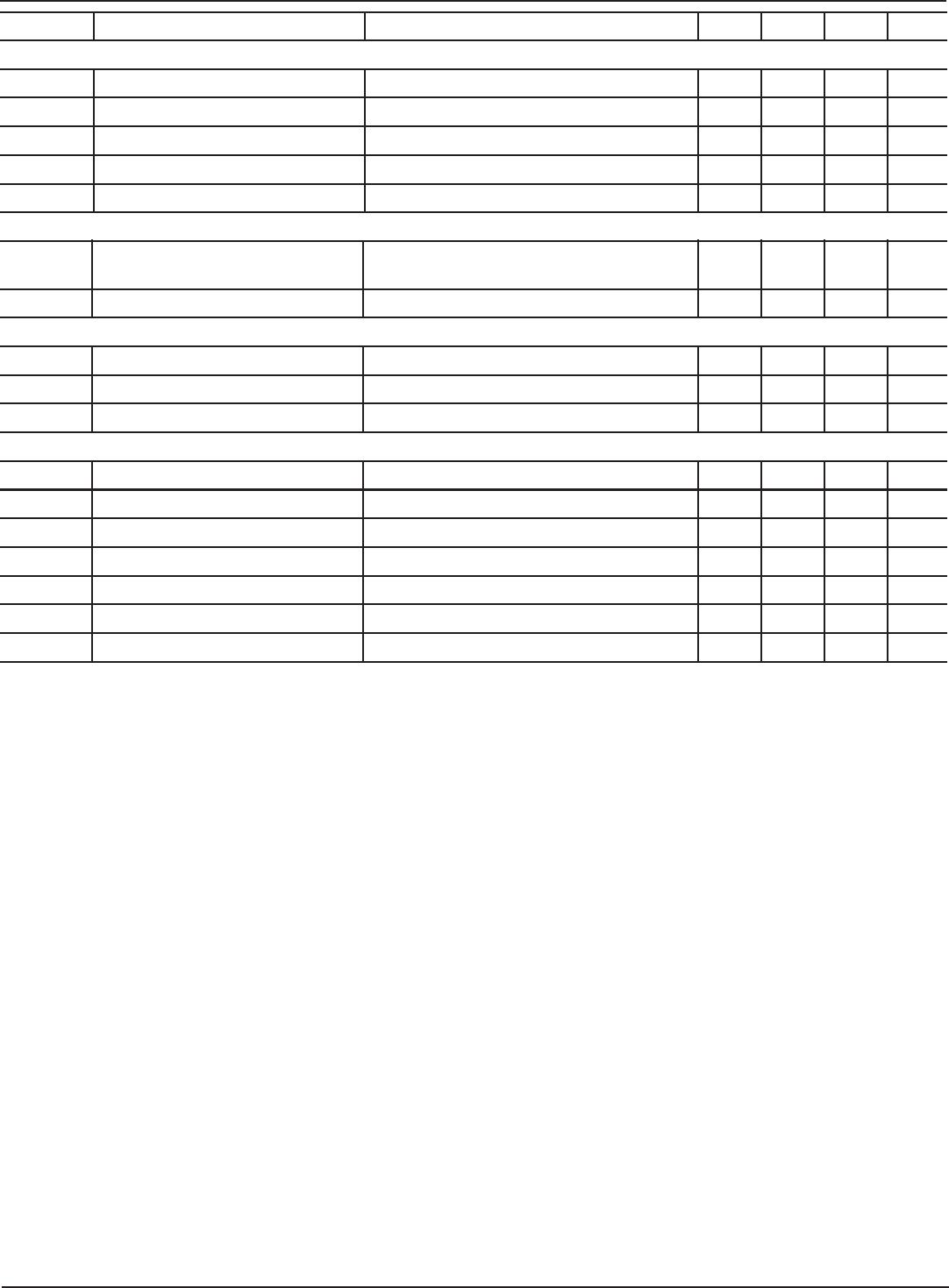
Electrical Characteristics
(4)
V
DD
= 3.3V ±10%
Symbol Parameter Test Condition Min Typ Max Units
Total Supply Current (including TX output driver current)
(5)
I
DD1
Normal 100BASE-TX Including 43mA output current 116 mA
I
DD2
Normal 10BASE-T (independent of Including 103mA output current 151 mA
utilization)
I
DD3
Power-Saving Mode 1 Auto-Negotiation is Enable 47 mA
I
DD5
Power-Down Mode 4mA
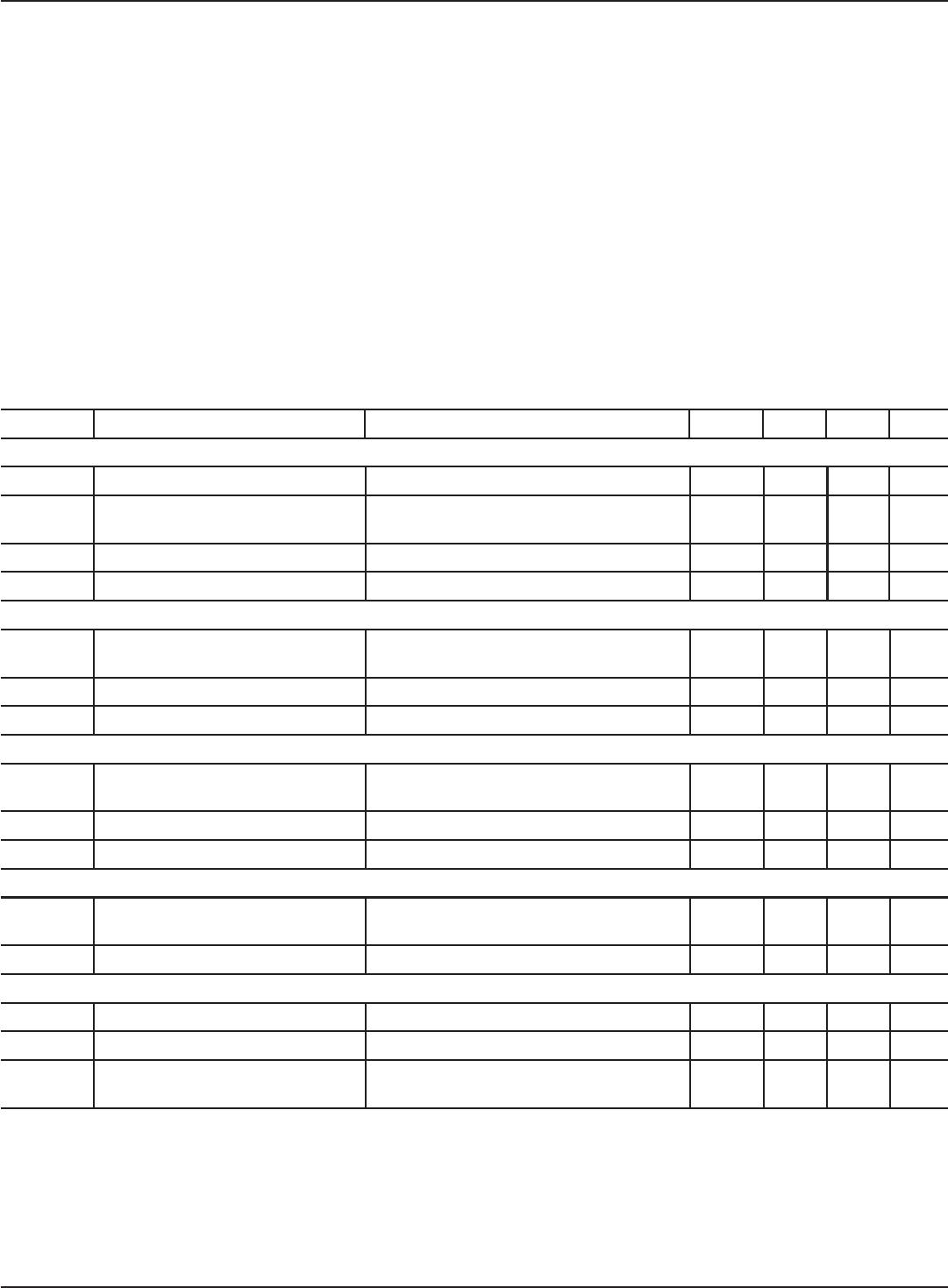
TTL Inputs
V
IH
Input High Voltage 1/2V
DD
(I/O) V
+0.2
V
IL
Input Low Voltage 0.8 V
I
IN
Input Current V
IN
= GND ~ V
DD
–10 10 µA
TTL Outputs
V
OH
Output High Voltage I
OH
= –4mA 1/2V
DD
(I/O) V
+0.6
V
OL
Output Low Voltage I
OL
= 4mA 0.4 V
|I
OZ
| Output Tri-State Leakage 10 µA
100BASE-TX Receive
R
IN
RX+/RX– Differential Input 8 kΩ
Resistance
Propagation Delay From magnetics to RDTX 50 110 ns
100BASE-TX Transmit (measured differentially after 1:1 transformer)
V
O
Peak Differential Output Voltage 50Ω from each output to V
DD
0.95 1.05 V
V
IMB
Output Voltage Imbalance 50Ω from each output to V
DD
2%
t
r
, t
t
Rise/Fall Time 35ns
Rise/Fall Time Imbalance 0 0.5 ns
Notes:
1. Exceeding the absolute maximum rating(s) may cause permanent damage to the device. Operating at maximum conditions for extended periods may
affect device reliability.
2. The device is not guaranteed to function outside its operating rating. Unused inputs must always be tied to an appropriate logic voltage level (Ground
to V
DD
).
3. No HS (heat spreader) in package.
4. Specification for packaged product only.
5. There is 100% data transmission in full-duplex mode and a minimum IPG with a 130-meter cable.
Absolute Maximum Ratings
(1)
Storage Temperature (T
S
) ....................... –55°C to +150°C
Supply Referenced to GND ........................ –0.5V to +4.0V
All Pins ........................................................ –0.5V to +4.0V
Important: Please read the Notes at the bottom of the
page.
Operating Ratings
(2)
Supply Voltage
(V
DD_PLL
,
V
DD_TX
,
V
DD_RXC
,
V
DD_RCV,
V
DDC
)........ +2.5V
(V
DDIO
) ...................................................................+3.3V
Ambient Temperature (T
A
)
Commercial ................................................ 0°C to +70°C
Industrial ................................................. –40°C to +85°C
Package Thermal Resistance
(3)
LQFP (θ
JA
)
No Airflow ................................................... 83.56°C/W