1
DATASHEET
Dual Supply/Low Power/1024-Tap/SPI Bus, Single
Digitally-Controlled (XDCP™) Potentiometer
X9110
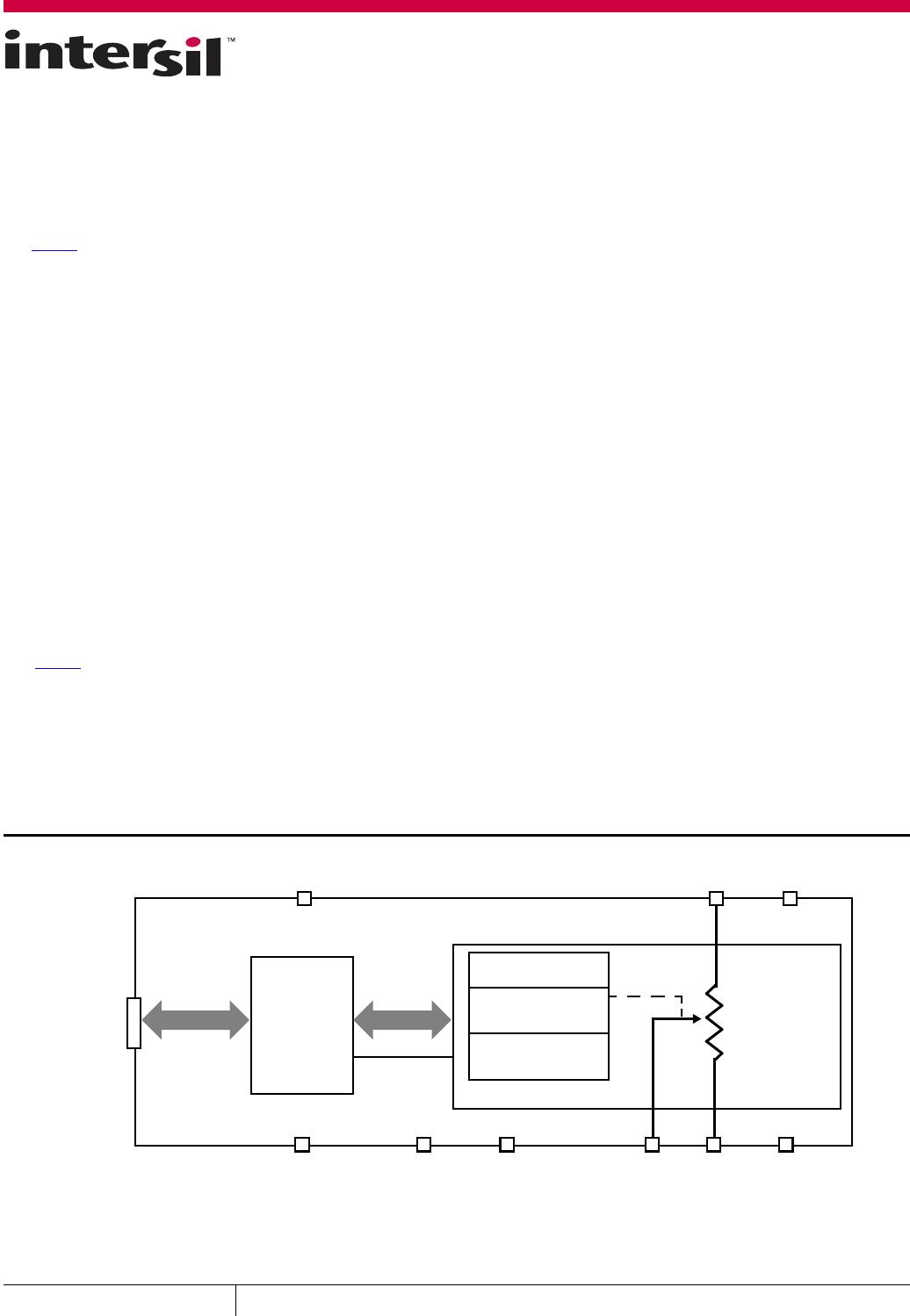
The X9110 integrates a Single Digitally Controlled
Potentiometer (XDCP) on a monolithic CMOS integrated circuit.
The digital controlled potentiometer is implemented using
1023 resistive elements in a series array. Between each
element are tap points connected to the wiper terminal
through switches. The position of the wiper on the array is
controlled by the user through the SPI bus interface. The
potentiometer has associated with it a volatile Wiper Counter
Register (WCR) and four nonvolatile data registers that can be
directly written to, and read by, the user. The contents of the
WCR controls the position of the wiper on the resistor array
though the switches. Power-up recalls the contents of the
default data register (DR0) to the WCR.
The XDCP can be used as a three-terminal potentiometer or as
a two terminal variable resistor in a wide variety of
applications including control, parameter adjustments, and
signal processing.
Related Literature
For a full list of related documents, visit our website
- X9110
product page
Features
1024 resistor taps – 10-bit resolution
SPI serial interface for write, read, and transfer operations of
the potentiometer
Wiper resistance, 40Ωtypical at 5V
Four nonvolatile data registers
Nonvolatile storage of multiple wiper positions
Power-on recall, loads saved wiper position on power-up
Standby current <5µA maximum
•System V
CC
: 2.7V to 5.5V operation
Analog V+/V-: -5V to +5V
100kΩend-to-end resistance
100 year data retention
Endurance: 100,000 data changes per bit per register
•14 Ld TSSOP
Dual supply version of the X9111
•Low power CMOS
Pb-free (RoHS compliant)
FIGURE 1. FUNCTIONAL DIAGRAM
R
H
R
L
BUS
R
W
INTERFACE
CONTROL
POT
V
CC
V
SS
SPI
BUS
ADDRESS
DATA
STATUS
WRITE
READ
WIPER
1024-TAPS
TRANSFER
NC NC
100kΩ
POWER-ON RECALL
WIPER COUNTER
REGISTER (WCR)
DATA REGISTERS
(DR0-DR3)
CONTROL
INTERFACE
V+
V-
AND
October 28, 2016
FN8158.5
CAUTION: These devices are sensitive to electrostatic discharge; follow proper IC Handling Procedures.
1-888-INTERSIL or 1-888-468-3774
| Copyright Intersil Americas LLC 2005, 2008, 2016. All Rights Reserved
Intersil (and design) and XDCP are trademarks owned by Intersil Corporation or one of its subsidiaries.
All other trademarks mentioned are the property of their respective owners.
X9110
2
FN8158.5
October 28, 2016
Submit Document Feedback
Applications
Circuit Level Applications
Vary the gain of a voltage amplifier
Provide programmable DC reference voltages for comparators
and detectors
Control the volume in audio circuits
Trim out the offset voltage error in a voltage amplifier circuit
Set the output voltage of a voltage regulator
Trim the resistance in Wheatstone bridge circuits
Control the gain, characteristic frequency and Q-factor in filter
circuits
Set the scale factor and zero point in sensor signal
conditioning circuits
Vary the frequency and duty cycle of timer ICs
Vary the DC biasing of a pin diode attenuator in RF circuits
Provide a control variable (I, V, or R) in feedback circuits
System Level Applications
Adjust the contrast in LCD displays
Control the power level of LED transmitters in communication
systems
Set and regulate the DC biasing point in an RF power amplifier
in wireless systems
Control the gain in audio and home entertainment systems
Provide the variable DC bias for tuners in RF wireless systems
Set the operating points in temperature control systems
Control the operating point for sensors in industrial systems
Trim offset and gain errors in artificial intelligent systems
Ordering Information
PART NUMBER
(Notes 2
, 3)
PART
MARKING
V
CC
LIMITS
(V)
POTENTIOMETER
RANGE (kΩ)
TEMP RANGE
(°C)
PACKAGE
(RoHS COMPLIANT) PKG. DWG. #
X9110TV14Z (Note 1
) X9110 TVZ 5 ±10 100 0 to +70 14 Ld TSSOP M14.173
X9110TV14IZ X9110 TVZI -40 to +85 14 Ld TSSOP M14.173
X9110TV14Z-2.7 X9110 TVZF 2.7 to 5.5 0 to +70 14 Ld TSSOP M14.173
X9110TV14IZ-2.7 (Note 1
) X9110 TVZG -40 to +85 14 Ld TSSOP M14.173
NOTES:
1. Add “T1” suffix for 2.5k unit tape and reel option.
2. These Intersil Pb-free plastic packaged products employ special Pb-free material sets, molding compounds/die attach materials, and 100% matte
tin plate plus anneal (e3 termination finish, which is RoHS compliant and compatible with both SnPb and Pb-free soldering operations). Intersil
Pb-free products are MSL classified at Pb-free peak reflow temperatures that meet or exceed the Pb-free requirements of IPC/JEDEC J STD-020.
3. For Moisture Sensitivity Level (MSL), see product information page for X9110
. For more information on MSL, see tech brief TB363.
X9110
3
FN8158.5
October 28, 2016
Submit Document Feedback
Bus Interface Pins
SERIAL OUTPUT (SO)
SO is a serial data output pin. During a read cycle, data is shifted
out on this pin. Data is clocked out on the falling edge of the
serial clock.
SERIAL INPUT (SI)
SI is the serial data input pin. All opcodes, byte addresses and
data to be written to the potentiometer pot registers are input on
this pin. Data is latched by the rising edge of the serial clock.
SERIAL CLOCK (SCK)
The SCK input is used to clock data into and out of the X9110.
HOLD (HOLD)
HOLD is used in conjunction with the CS pin to select the device.
Once the part is selected and a serial sequence is underway,
HOLD
may be used to pause the serial communication with the
controller without resetting the serial sequence. To pause, HOLD
must be brought LOW while SCK is LOW. To resume
communication, HOLD
is brought HIGH, again while SCK is LOW.
Detailed Functional Diagram
FIGURE 2. DETAILED FUNCTIONAL DIAGRAM
CS
SCK
A0
SO
SI
HOLD
WP
INTERFACE
AND
CONTROL
CIRCUITRY
V-
V+
V
CC
V
SS
DR0 DR1
DR2 DR3
WIPER
COUNTER
REGISTER
(WCR)
R
H
R
L
DATA
R
W
1024-TAPS
100kΩ
CONTROL
POWER ON
RECALL
Pin Configuration
X9110
14 LD TSSOP
TOP VIEW
Pin Descriptions
PIN
(TSSOP) SYMBOL FUNCTION
1 V+ Analog Supply Voltage
2 SO Serial Data Output
3 A0 Device Address
4 SCK Serial Clock
5WP
Hardware Write Protect
6 SI Serial Data Input
7V
SS
System Ground
8 V- Analog Supply Voltage
9CS
Chip Select
10 HOLD Device Select. Pause the Serial Bus
V
CC
R
L
V
SS
1
2
3
4
5
6
7
8
14
13
12
11
10
9
A0
R
W
SCK
CS
R
H
SO
V+
SI
HOLD
WP
V-
11 R
W
Wiper Terminal of the Potentiometer
12 R
H
High Terminal of the Potentiometer
13 R
L
Low Terminal of the Potentiometer
14 V
CC
System Supply Voltage
Pin Descriptions (Continued)
PIN
(TSSOP) SYMBOL FUNCTION

X9110TV14IZ-2.7

Mfr. #:
Manufacturer:
Renesas / Intersil
Description:
Digital Potentiometer ICs SINGLE DCP 100KOHM 1024 TAP SPI
Lifecycle:
New from this manufacturer.
Delivery:
DHL FedEx Ups TNT EMS
Payment:
T/T Paypal Visa MoneyGram Western Union