Expand menu
Hello, Sign in
My Account
0
Cart
Home
Products
Sensors
Semiconductors
Passive Components
Connectors
Power
Electromechanical
Optoelectronics
Circuit Protection
Integrated Circuits - ICs
Main Products
Manufacturers
Blog
Services
About OMO
About Us
Contact Us
Check Stock
X9110TV14IZ-2.7
P1-P3
P4-P6
P7-P9
P10-P12
P13-P15
P16-P18
X9110
13
FN81
58
.5
October 28, 201
6
Submit Document Feedback
Symbol T
able
XDCP Timing
SYMBOL
P
ARAMETER
MIN
MAX
UNIT
t
WRPO
Wiper Response Time After the Third (Last
) Power Supply is
Stable
5
10
µs
t
WRL
Wiper Response T
ime After Instruction Issued (All Load Instructions)
5
10
µs
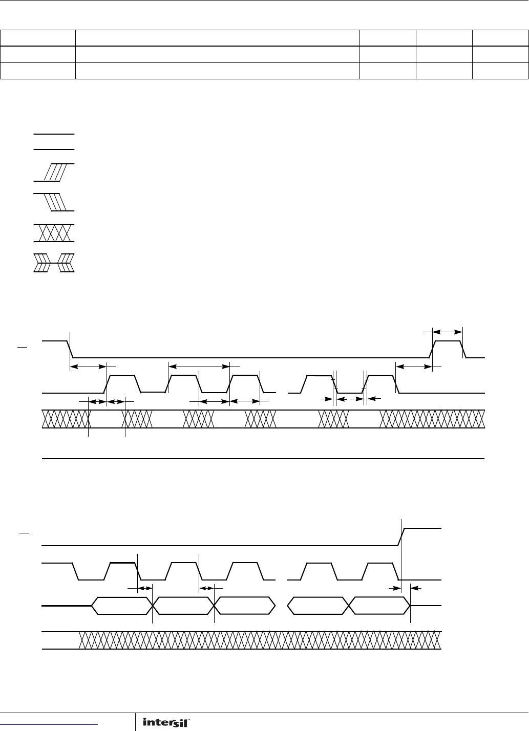
WAVEFORM
INPUTS
OUTP
UTS
Must be
steady
Will be
steady
May change
from LOW to
HIGH
Will chan
ge
from LOW
to
HIGH
May change
from HIGH to
LOW
Will chan
ge
from HIGH t
o
LOW
Don’t Care:
Changes
Allowed
Changing:
State Not
Kno
wn
N/A
Center Line
is High
Impedance
Timing Diagrams
FIGURE 7
.
INPUT TIMING
FIGURE 8.
OUTP
UT TIMING
...
CS
SCK
SI
SO
MSB
LSB
HIGH IMPEDANCE
t
LEAD
t
H
t
SU
t
FI
t
CS
t
LAG
t
CYC
t
WL
...
t
RI
t
WH
...
CS
SCK
SO
SI
ADDR
MSB
LSB
t
DIS
t
HO
t
V
...
X9110
14
FN81
58
.5
October 28, 201
6
Submit Document Feedback
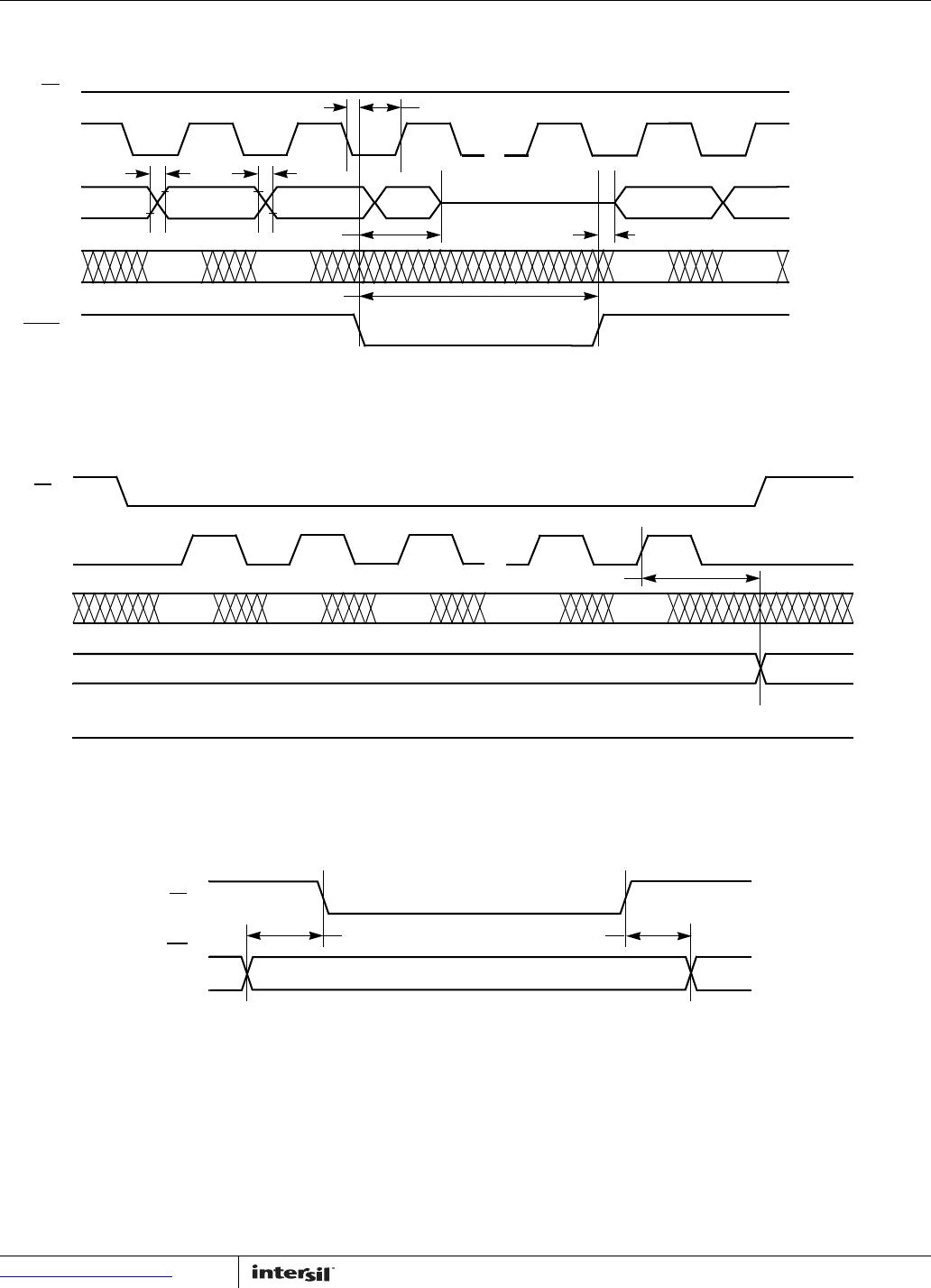
FIGURE 9.
HOLD TIMING
FIGURE 10.
XD
CP TIMING (FOR ALL LOAD INSTRUCTIONS)
FIGURE 11.
WRITE PRO
TECT AND DEVICE ADDRESS PINS
TIMING
Timing Diagrams
(Continued)
...
CS
SCK
SO
SI
HOLD
t
HSU
t
HH
t
LZ
t
HZ
t
HOLD
t
RO
t
FO
...
CS
SCK
SI
MSB
LSB
R
W
t
WRL
...
SO
HIGH IMPEDANCE
CS
WP
A0
A1
t
WP
ASU
t
WP
AH
(ANY INSTRUCTION)
X9110
15
FN81
58
.5
October 28, 201
6
Submit Document Feedback
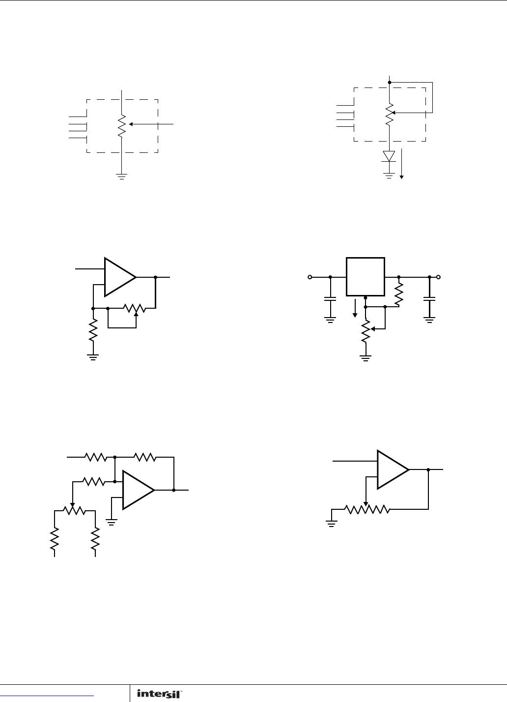
Applications information
Basic Configurations of Electronic Potentiometers
FIGURE 12.
THREE TERMINAL POTENTIOMETER;
V
ARIABLE V
O
L
T
AGE DI
VIDER
FIGURE 13.
T
WO TERMIN
AL VARIABLE R
ESISTOR;
V
ARIABLE CURRENT
V
R
RW
+V
R
I
Application Circuits
FIGURE 14.
NONINVERTING AMPLIFIER
FIGURE 15.
VOL
T
AGE REGULA
TOR
FIGURE 16.
OFFSET VOL
T
AGE ADJUSTMENT
FIGURE 1
7
.
COMPARA
TOR WITH HYSTERESIS
+
–
V
S
V
O
R
2
R
1
V
O
= (1+R
2
/R
1
)V
S
R
1
R
2
I
adj
V
O
(REG)
V
IN
317
V
O
(REG) = 1.25V (1+R
2
/R
1
)+I
adj
R
2
+
–
V
S
V
O
R
2
R
1
100kΩ
10kΩ
10kΩ
10kΩ
-12V
+12V
TL072
+
–
V
S
V
O
R
2
R
1
}
}
V
UL
= {R
1
/(R
1
+R
2
)} V
O
(max)
RL
L
= {R
1
/(R
1
+R
2
)} V
O
(min)
P1-P3
P4-P6
P7-P9
P10-P12
P13-P15
P16-P18
X9110TV14IZ-2.7
Mfr. #:
Buy X9110TV14IZ-2.7
Manufacturer:
Renesas / Intersil
Description:
Digital Potentiometer ICs SINGLE DCP 100KOHM 1024 TAP SPI
Lifecycle:
New from this manufacturer.
Delivery:
DHL
FedEx
Ups
TNT
EMS
Payment:
T/T
Paypal
Visa
MoneyGram
Western
Union
Products related to this Datasheet
X9110TV14Z-2.7
X9110TV14IZ-2.7
X9110TV14ZT1
X9110TV14IZ-2.7T1
X9110TV14IZ
X9110TV14
X9110TV14-2.7
X9110TV14I
X9110TV14I-2.7