1
LTC3410B
3410bfa
■
High Efficiency: Up to 96%
■
300mA Output Current at V
IN
= 3V
■
380mA Minimum Peak Switch Current
■
2.5V to 5.5V Input Voltage Range
■
2.25MHz Constant Frequency Operation
■
No Schottky Diode Required
■
Low Dropout Operation: 100% Duty Cycle
■
Stable with Ceramic Capacitors
■
0.8V Reference Allows Low Output Voltages
■
Shutdown Mode Draws < 1µA Supply Current
■
±2% Output Voltage Accuracy
■
Current Mode Operation for Excellent Line and
Load Transient Response
■
Overtemperature Protected
■
Available in Low Profile SC70 Package
The LTC
®
3410B is a high efficiency monolithic synchro-
nous buck regulator using a constant frequency, current
mode architecture. The device is available in adjustable
and fixed output voltage versions. Supply current during
operation is only 200µA, dropping to <1µA in shutdown.
The 2.5V to 5.5V input voltage range makes the LTC3410B
ideally suited for single Li-Ion battery-powered applica-
tions. 100% duty cycle provides low dropout operation,
extending battery life in portable systems. PWM pulse
skipping mode operation provides very low output ripple
voltage for noise sensitive applications.
Switching frequency is internally set at 2.25MHz, allowing
the use of small surface mount inductors and capacitors.
The LTC3410B is specifically designed to work well with
ceramic output capacitors, achieving very low output
voltage ripple and a small PCB footprint.
The internal synchronous switch increases efficiency and
eliminates the need for an external Schottky diode. Low
output voltages are easily supported with the 0.8V feed-
back reference voltage. The LTC3410B is available in a
tiny, low profile SC70 package.
■
Cellular Telephones
■
Personal Information Appliances
■
Wireless and DSL Modems
■
Digital Still Cameras
■
MP3 Players
■
Portable Instruments
2.25MHz, 300mA
Synchronous Step-Down
Regulator in SC70
APPLICATIO S
U
FEATURES
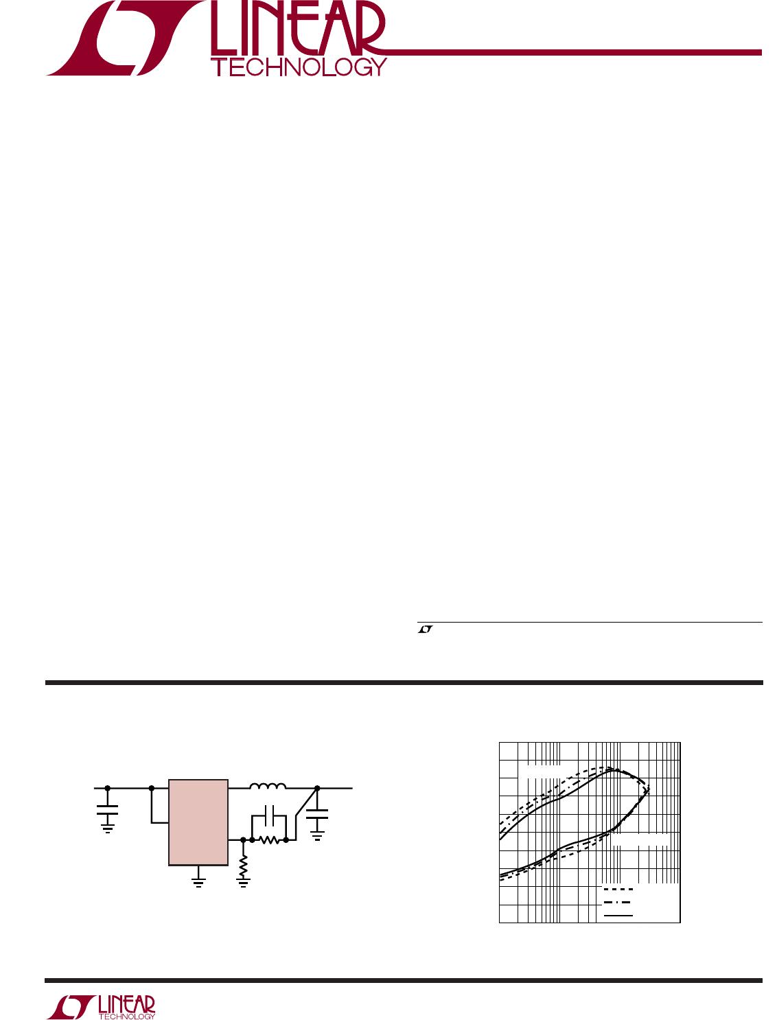
TYPICAL APPLICATIO
U
DESCRIPTIO
U
Efficiency and Power Loss
vs Output Current
V
IN
C
IN
2.2µF
CER
V
IN
2.7V
TO 5.5V
LTC3410B
RUN
4.7µH
10pF
232k
464k
3410 TA01
SW
V
FB
GND
C
OUT
2.2µF
CER
V
OUT
1.2V
POWER LOSS (W)
1
0.1
0.01
0.001
0.0001
OUTPUT CURRENT (mA)
1
40
EFFICIENCY (%)
50
60
70
80
10 100
1000
3410 TA01b
30
20
20
0
90
100
EFFICIENCY
POWER LOSS
V
IN
= 2.7V
V
IN
= 3.6V
V
IN
= 4.2V
, LT, LTC and LTM are registered trademarks of Linear Technology Corporation. All
other trademarks are the property of their respective owners. Protected by U.S. Patents,
including 5481178, 5994885, 6580258, 6304066, 6127815, 6498466, 6611131.