LTC3410BESC6-1.875#TRMPBF

10
LTC3410B
3410bfa
APPLICATIO S I FOR ATIO
WUUU
Efficiency Considerations
The efficiency of a switching regulator is equal to the
output power divided by the input power times 100%. It is
often useful to analyze individual losses to determine what
is limiting the efficiency and which change would produce
the most improvement. Efficiency can be expressed as:
Efficiency = 100% – (L1 + L2 + L3 + ...)
where L1, L2, etc. are the individual losses as a percentage
of input power.
Although all dissipative elements in the circuit produce
losses, two main sources usually account for most of the
losses in LTC3410B circuits: V
IN
quiescent current and I
2
R
losses. The V
IN
quiescent current loss dominates the
efficiency loss at very low load currents whereas the I
2
R
loss dominates the efficiency loss at medium to high load
currents. In a typical efficiency plot, the efficiency curve at
very low load currents can be misleading since the actual
power lost is of no consequence as illustrated in Figure 3.
1. The V
IN
quiescent current is due to two components:
the DC bias current as given in the electrical character-
istics and the internal main switch and synchronous
switch gate charge currents. The gate charge current
results from switching the gate capacitance of the
internal power MOSFET switches. Each time the gate is
switched from high to low to high again, a packet of
charge, dQ, moves from V
IN
to ground. The resulting
dQ/dt is the current out of V
IN
that is typically larger than
the DC bias current. In continuous mode,
I
GATECHG
= f(Q
T
+ Q
B
) where Q
T
and Q
B
are the
gate charges of the internal top and bottom
switches. Both the DC bias and gate charge
losses are proportional to V
IN
and thustheir effectswill
be more pronounced at higher supply voltages.
2. I
2
R losses are calculated from the resistances of the
internal switches, R
SW
, and external inductor R
L
. In
continuous mode, the average output current flowing
through inductor L is “chopped” between the main
switch and the synchronous switch. Thus, the series
resistance looking into the SW pin is a function of both
top and bottom MOSFET R
DS(ON)
and the duty cycle
(DC) as follows:
R
SW
= (R
DS(ON)TOP
)(DC) + (R
DS(ON)BOT
)(1 – DC)
The R
DS(ON)
for both the top and bottom MOSFETs can
be obtained from the Typical Performance Charateristics
curves. Thus, to obtain I
2
R losses, simply add R
SW
to
R
L
and multiply the result by the square of the average
output current.
Other losses including C
IN
and C
OUT
ESR dissipative
losses and inductor core losses generally account for less
than 2% total additional loss.
Figure 3. Power Lost vs Load Current
LOAD CURRENT (mA)
0.1 1
0.0001
POWER LOST (W)
0.01
1
10 100 1000
3410 F03
0.001
0.1
V
OUT
= 1.2V
V
OUT
= 1.8V
V
OUT
= 2.5V
11
LTC3410B
3410bfa
APPLICATIO S I FOR ATIO
WUUU
Thermal Considerations
In most applications the LTC3410B does not dissipate
much heat due to its high efficiency. But, in applications
where the LTC3410B is running at high ambient
temperature with low supply voltage and high duty
cycles, such as in dropout, the heat dissipated may
exceed the maximum junction temperature of the part. If
the junction temperature reaches approximately 150°C,
both power switches will be turned off and the SW node
will become high impedance.
To avoid the LTC3410B from exceeding the maximum
junction temperature, the user will need to do some
thermal analysis. The goal of the thermal analysis is to
determine whether the power dissipated exceeds the
maximum junction temperature of the part. The tempera-
ture rise is given by:
T
R
= (P
D
)(θ
JA
)
where P
D
is the power dissipated by the regulator and
θ
JA
is the thermal resistance from the junction of the die to
the ambient temperature.
The junction temperature, T
J
, is given by:
T
J
= T
A
+ T
R
where T
A
is the ambient temperature.
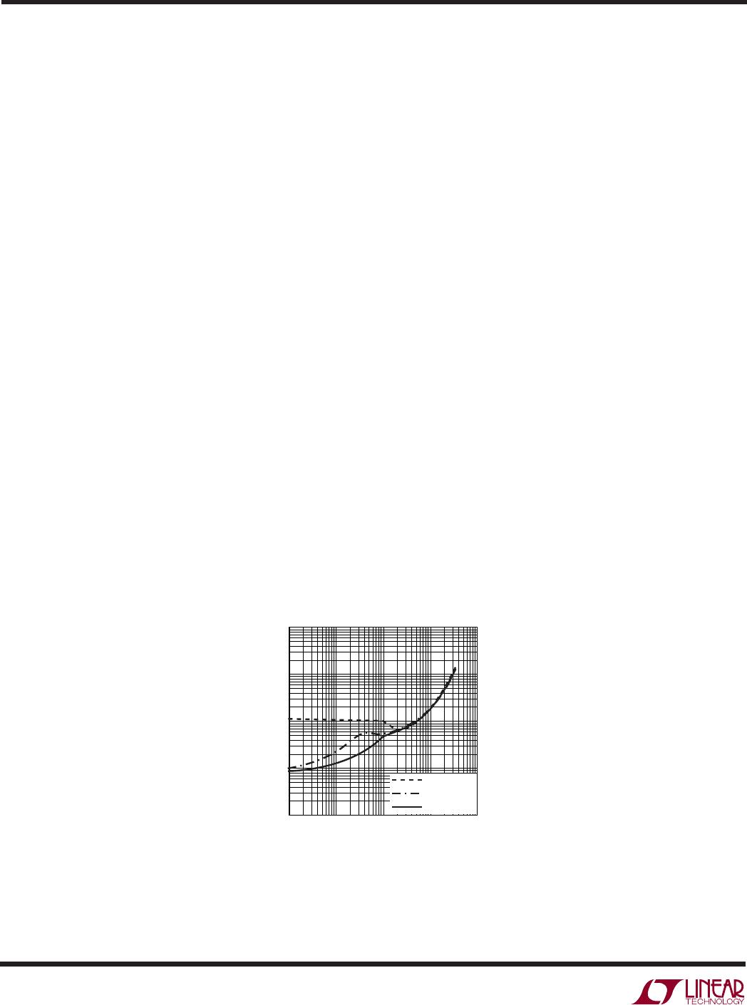
As an example, consider the LTC3410B in dropout at an
input voltage of 2.7V, a load current of 300mA and an
ambient temperature of 70°C. From the typical perfor-
mance graph of switch resistance, the R
DS(ON)
of the
P-channel switch at 70°C is approximately 1.0.
Therefore, power dissipated by the part is:
P
D
= I
LOAD
2
• R
DS(ON)
= 90mW
For the SC70 package, the θ
JA
is 250°C/W. Thus, the
junction temperature of the regulator is:
T
J
= 70°C + (90)(250) = 92.5°C
which is well below the maximum junction temperature
of 125°C.
Note that at higher supply voltages, the junction tempera-
ture is lower due to reduced switch resistance (R
DS(ON)
).
Checking Transient Response
The regulator loop response can be checked by looking at
the load transient response. Switching regulators take
several cycles to respond to a step in load current. When
a load step occurs, V
OUT
immediately shifts by an amount
equal to (I
LOAD
• ESR), where ESR is the effective series
resistance of C
OUT
. I
LOAD
also begins to charge or
discharge C
OUT
, which generates a feedback error signal.
The regulator loop then acts to return V
OUT
to its steady-
state value. During this recovery time V
OUT
can be moni-
tored for overshoot or ringing that would indicate a stability
problem. For a detailed explanation of switching control
loop theory, see Application Note 76.
A second, more severe transient is caused by switching in
loads with large (>1µF) supply bypass capacitors. The
discharged bypass capacitors are effectively put in parallel
with C
OUT
, causing a rapid drop in V
OUT
. No regulator can
deliver enough current to prevent this problem if the load
switch resistance is low and it is driven quickly. The only
solution is to limit the rise time of the switch drive so that
the load rise time is limited to approximately (25 • C
LOAD
).
Thus, a 10µF capacitor charging to 3.3V would require a
250µs rise time, limiting the charging current to about
130mA.
12
LTC3410B
3410bfa
APPLICATIO S I FOR ATIO
WUUU
PC Board Layout Checklist
When laying out the printed circuit board, the following
checklist should be used to ensure proper operation of the
LTC3410B. These items are also illustrated graphically in
Figures 4 and 5. Check the following in your layout:
1. The power traces, consisting of the GND trace, the SW
trace and the V
IN
trace should be kept short, direct and
wide.
2. Does the V
FB
pin connect directly to the feedback
resistors? The resistive divider R1/R2 must be con-
nected between the (+) plate of C
OUT
and ground.
3. Does the (+) plate of C
IN
connect to V
IN
as closely as
possible? This capacitor provides the AC current to the
internal power MOSFETs.
4. Keep the (–) plates of C
IN
and C
OUT
as close as possible.
5. Keep the switching node, SW, away from the sensitive
V
FB
node.
Figure 4a. LTC3410B Layout Diagram
Figure 5a. LTC3410B Suggested Layout
RUN
LTC3410B
GND
SW
L1
R2
R1
C
FWD
BOLD LINES INDICATE HIGH CURRENT PATHS
V
IN
V
OUT
3410B F04a
4
6
5
1
3
+
2
V
FB
V
IN
C
IN
C
OUT
LTC3410B
GND
3410B F05a
PIN 1
V
OUT
V
IN
VIA TO V
OUT
SW
VIA TO V
IN
VIA TO GND
C
OUT
C
IN
L1
R2
C
FWD
R1
RUN
LTC3410B-1.875
GND
SW
L1
BOLD LINES INDICATE HIGH CURRENT PATHS
V
IN
V
OUT
3410B F04b
4
6
5
1
3
+
2
V
OUT
V
IN
C
IN
C
OUT
Figure 4b. LTC3410B-1.875 Layout Diagram
LTC3410B-
1.875
3410B F05b
PIN 1
V
OUT
V
IN
SW
VIA TO V
IN
C
OUT
C
IN
L1
Figure 5b. LTC3410B Fixed Output Voltage
Suggested Layout

LTC3410BESC6-1.875#TRMPBF

Mfr. #:
Manufacturer:
Analog Devices / Linear Technology
Description:
Switching Voltage Regulators 1.875V, 300mA, 2.25MHz Synch Step-Dwn in SC70
Lifecycle:
New from this manufacturer.
Delivery:
DHL FedEx Ups TNT EMS
Payment:
T/T Paypal Visa MoneyGram Western Union