LTC3410BESC6-1.875#TRMPBF

13
LTC3410B
3410bfa
APPLICATIO S I FOR ATIO
WUUU
Design Example
As a design example, assume the LTC3410B is used in a
single lithium-ion battery-powered cellular phone
application. The V
IN
will be operating from a maximum of
4.2V down to about 2.7V. The load current requirement
is a maximum of 0.3A but most of the time it will be in
standby mode, requiring only 2mA. Efficiency at both low
and high load currents is important. Output voltage is
2.5V. With this information we can calculate L using
Equation (1),
L
fI
V
V
V
L
OUT
OUT
IN
=
()
()
1
1
(3)
Substituting V
OUT
= 2.5V, V
IN
= 4.2V, I
L
= 100mA
and f = 2.25MHz in Equation (3) gives:
L
V
MHz mA
V
V
H=
=
25
2 25 100
1
25
42
45
.
.()
.
.
. µ
For best efficiency choose a 300mA or greater inductor
with less than 0.3 series resistance.
C
IN
will require an RMS current rating of at least 0.125A
I
LOAD(MAX)
/2 at temperature and C
OUT
will require an ESR
of less than 0.5. In most cases, a ceramic capacitor will
satisfy this requirement.
For the feedback resistors, choose R1 = 412k. R2 can
then be calculated from equation (2) to be:
R
V
R k use
OUT
2
08
1 1 875 5 8=
=
.
. ; 87k
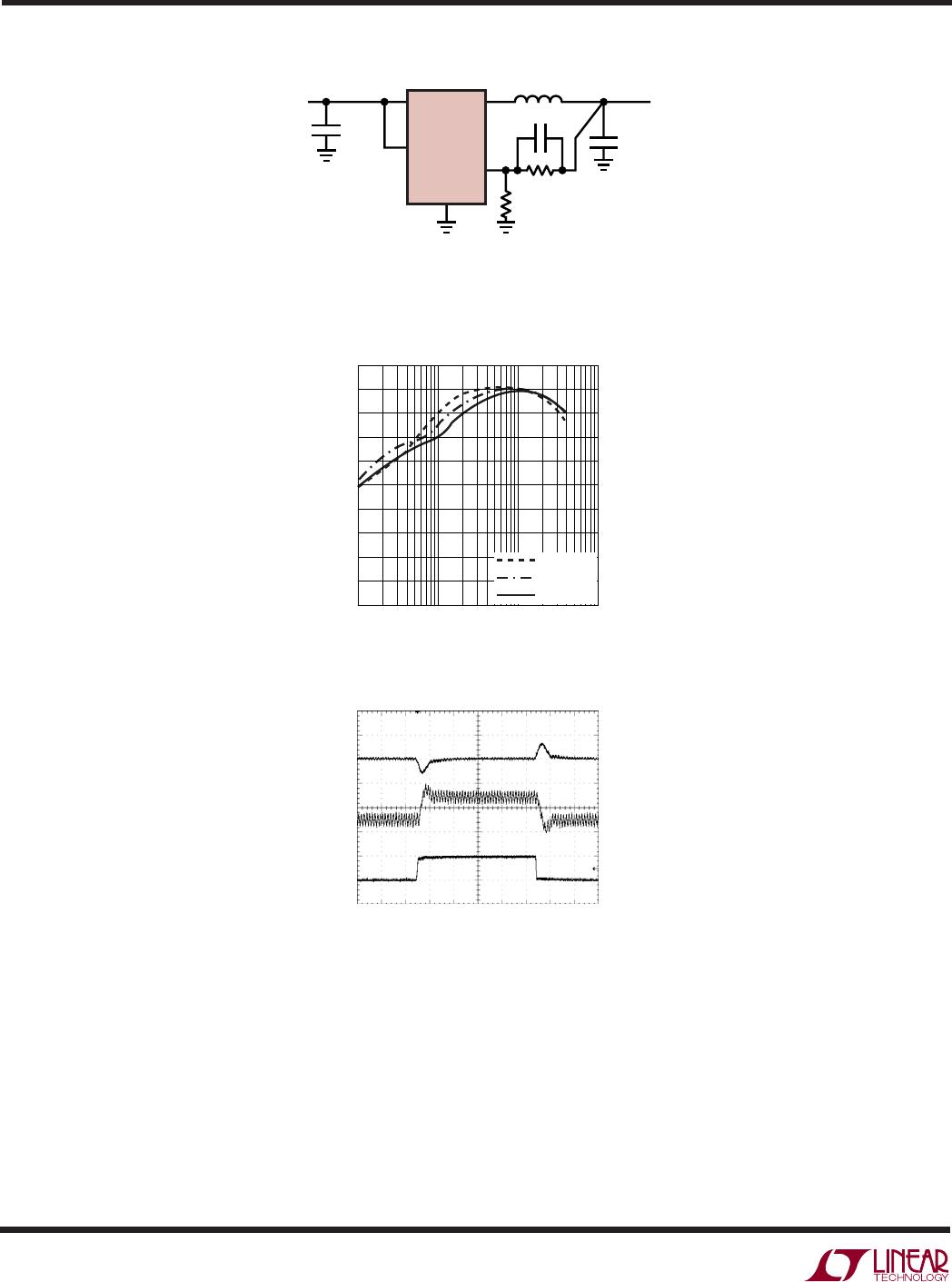
Figure 6 shows the complete circuit along with its
efficiency curve.
Figure 6a
Figure 6b Figure 6c
V
IN
C
IN
2.2µF
CER
V
IN
2.7V
TO 4.2V
LTC3410B
RUN
3
4.7µH*
10pF
887k
412k
3410 F07a
6
4
1
2, 5
SW
V
FB
GND
C
OUT
2.2µF
CER
V
OUT
2.5V
TAIYO YUDEN JMK212BJ225
*MURATA LQH32CN4R7M23
OUTPUT CURRENT (mA)
1
40
EFFICIENCY (%)
50
60
70
80
10 100 1000
3410 F07b
30
20
10
0
90
100
V
IN
= 2.7V
V
IN
= 3.6V
V
IN
= 4.2V
4µs/DIV
V
OUT
100mV/DIV
AC COUPLED
V
IN
= 3.6V
V
OUT
= 2.5V
I
LOAD
= 100mA TO 300mA
I
LOAD
200mA/DIV
I
L
200mA/DIV
3410 F07c
14
LTC3410B
3410bfa
U
TYPICAL APPLICATIO
V
IN
C
IN
2.2µF
V
IN
2.7V
TO 4.2V
LTC3410B
RUN
3
4.7µH*
10pF
402k
464k
3410 TA02
6
4
1
2, 5
SW
V
FB
GND
C
OUT
2.2µF
V
OUT
1.5V
TAIYO YUDEN JMK212BJ225
*MURATA LQH32CN4R7M23
4µs/DIV
V
OUT
100mV/DIV
AC COUPLED
V
IN
= 3.6V
V
OUT
= 1.5V
I
LOAD
= 100mA TO 250mA
I
LOAD
200mA/DIV
IL
200mA/DIV
3410 TA04
3410 TA03
OUTPUT CURRENT (mA)
1
40
EFFICIENCY (%)
50
60
70
80
10 100 1000
30
20
10
0
90
100
V
IN
= 2.7V
V
IN
= 3.6V
V
IN
= 4.2V
15
LTC3410B
3410bfa
Information furnished by Linear Technology Corporation is believed to be accurate and reliable.
However, no responsibility is assumed for its use. Linear Technology Corporation makes no represen-
tation that the interconnection of its circuits as described herein will not infringe on existing patent rights.
U
PACKAGE DESCRIPTIO
SC6 Package
6-Lead Plastic SC70
(Reference LTC DWG # 05-08-1638)
1.15 – 1.35
(NOTE 4)
1.80 – 2.40
0.15 – 0.30
6 PLCS (NOTE 3)
SC6 SC70 1205 REV B
1.80 – 2.20
(NOTE 4)
0.65 BSC
PIN 1
0.80 – 1.00
1.00 MAX
0.00 – 0.10
REF
NOTE:
1. DIMENSIONS ARE IN MILLIMETERS
2. DRAWING NOT TO SCALE
3. DIMENSIONS ARE INCLUSIVE OF PLATING
4. DIMENSIONS ARE EXCLUSIVE OF MOLD FLASH AND METAL BURR
5. MOLD FLASH SHALL NOT EXCEED 0.254mm
6. DETAILS OF THE PIN 1 IDENTIFIER ARE OPTIONAL,
BUT MUST BE LOCATED WITHIN THE INDEX AREA
7. EIAJ PACKAGE REFERENCE IS EIAJ SC-70
8. JEDEC PACKAGE REFERENCE IS MO-203 VARIATION AB
2.8 BSC
0.47
MAX
0.65
REF
RECOMMENDED SOLDER PAD LAYOUT
PER IPC CALCULATOR
1.8 REF
1.00 REF
INDEX AREA
(NOTE 6)
0.10 – 0.18
(NOTE 3)
0.26 – 0.46
GAUGE PLANE
0.15 BSC
0.10 – 0.40

LTC3410BESC6-1.875#TRMPBF

Mfr. #:
Manufacturer:
Analog Devices / Linear Technology
Description:
Switching Voltage Regulators 1.875V, 300mA, 2.25MHz Synch Step-Dwn in SC70
Lifecycle:
New from this manufacturer.
Delivery:
DHL FedEx Ups TNT EMS
Payment:
T/T Paypal Visa MoneyGram Western Union