AD7390ARZ-REEL7

REV. A
Information furnished by Analog Devices is believed to be accurate and
reliable. However, no responsibility is assumed by Analog Devices for its
use, nor for any infringements of patents or other rights of third parties that
may result from its use. No license is granted by implication or otherwise
under any patent or patent rights of Analog Devices.
a
AD7390/AD7391
One Technology Way, P.O. Box 9106, Norwood, MA 02062-9106, U.S.A.
Tel: 781/329-4700 www.analog.com
Fax: 781/326-8703 © Analog Devices, Inc., 2002
3 V Serial-Input
Micropower 10-Bit and 12-Bit DACs
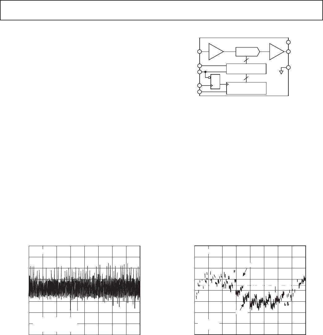
FUNCTIONAL BLOCK DIAGRAM
EN
AD7390
DAC REGISTER
12-BIT DAC
12
12
SERIAL REGISTER
REF
V
DD
CLR
LD
CLK
SDI
GND
V
OUT
FEATURES
Micropower—100 A
Single-Supply—2.7 V to 5.5 V Operation
Compact 1.75 mm Height SO-8 Package
and 1.1 mm Height TSSOP-8 Package
AD7390—12-Bit Resolution
AD7391—10-Bit Resolution
SPI and QSPI Serial Interface Compatible with Schmitt
Trigger Inputs
APPLICATIONS
Automotive 0.5 V to 4.5 V Output Span Voltage
Portable Communications
Digitally Controlled Calibration
GENERAL DESCRIPTION
The AD7390/AD7391 family of 10-bit and 12-bit voltage-
output digital-to-analog converters is designed to operate
from a single 3 V supply. Built using a CBCMOS process,
these monolithic DACs offer the user low cost, and ease-of-use
in single-supply 3 V systems. Operation is guaranteed over the
supply voltage range of 2.7 V to 5.5 V consuming less than 100 µA
making this device ideal for battery operated applications.
The full-scale voltage output is determined by the external
reference input voltage applied. The rail-to-rail REF
IN
to
DAC
OUT
allows for a full-scale voltage set equal to the positive
supply V
DD
or any value in between.
A doubled-buffered serial-data interface offers high-speed,
3-wire, SPI and microcontroller compatible inputs using data
in (SDI), clock (CLK) and load strobe (LD) pins. Addition-
ally, a CLR input sets the output to zero scale at power on or
upon user demand.
Both parts are offered in the same pinout to allow users to select
the amount of resolution appropriate for their application without
circuit card redesign.
The AD7390/AD7391 are specified over the extended industrial
(40°C to 85°C) temperature range. The AD7391AR is
specified for the 40°C to 125°C automotive temperature
range. The AD7390/AD7391s are available in plastic DIP, and
low profile 1.75 mm height SO-8 surface mount packages. The
AD7391ARU is available for ultracompact applications in a thin
1.1 mm TSSOP-8 package.
CODE – Decimal
1.00
1.00
0 4096512
DNL – LSB
1024 1536 2048 2560 3072 3584
0.75
0.00
0.25
0.50
0.75
0.50
0.25
AD7390
V
DD
= 3.0V
T
A
= 55C, +25C, +85C
SUPERIMPOSED
Figure 1. Differential Nonlinearity Error vs. Code
AD7390
V
DD
= 3.0V
V
REF
= 2.5V
+25C, +85C
CODE Decimal
0 4096512 1024 1536 2048 2560 3072 2584
2.0
2.0
INL LSB
1.5
0.0
0.5
1.0
1.5
1.0
0.5
55C
Figure 2. INL Error vs. Code and Temperature
REV. A
–2–
AD7390/AD7391–SPECIFICATIONS
Parameter Symbol Conditions 3 V 10% 5 V 10% Unit
STATIC PERFORMANCE
Resolution
1
N 12 12 Bits
Relative Accuracy
2
INL T
A
= 25°C ±1.6 ±1.6 LSB max
INL T
A
= 40°C, 85°C ±2.0 ±2 LSB max
Differential Nonlinearity
2
DNL T
A
= 25°C, Monotonic ±0.9 ±0.9 LSB max
DNL Monotonic ±1 ±1 LSB max
Zero-Scale Error V
ZSE
Data = 000
H
4.0 4.0 mV max
Full-Scale Voltage Error V
FSE
T
A
= 25°C, 85°C, Data = FFF
H
±8 ±8mV max
V
FSE
T
A
= 40°C, Data = FFF
H
±20 ±20 mV max
Full-Scale Tempco
3
TCV
FS
16 16 ppm/°C typ
REFERENCE INPUT
V
REF IN
Range V
REF
0/V
DD
0/V
DD
V min/max
Input Resistance R
REF
2.5 2.5 M typ
4
Input Capacitance
3
C
REF
5 5 pF typ
ANALOG OUTPUT
Output Current (Source) I
OUT
Data = 800
H
, V
OUT
= 5 LSB 1 1 mA typ
Output Current (Sink) I
OUT
Data = 800
H
, V
OUT
= 5 LSB 3 3 mA typ
Capacitive Load
3
C
L
No Oscillation 100 100 pF typ
LOGIC INPUTS
Logic Input Low Voltage V
IL
0.5 0.8 V max
Logic Input High Voltage V
IH
V
DD
0.6 V
DD
0.6 V min
Input Leakage Current I
IL
10 10 µA max
Input Capacitance
3
C
IL
10 10 pF max
INTERFACE TIMING
3, 5
Clock Width High t
CH
50 30 ns min
Clock Width Low t
CL
50 30 ns min
Load Pulsewidth t
LDW
30 20 ns min
Data Setup t
DS
10 10 ns min
Data Hold t
DH
30 15 ns min
Clear Pulsewidth t
CLRW
15 15 ns min
Load Setup t
LD1
30 15 ns min
Load Hold t
LD2
40 20 ns min
AC CHARACTERISTICS
6
Output Slew Rate SR Data = 000
H
to FFF
H
to 000
H
0.05 0.05 V/µs typ
Settling Time t
S
To 0.1% of Full Scale 70 60 µs typ
DAC Glitch Q Code 7FF
H
to 800
H
to 7FF
H
65 65 nVs typ
Digital Feedthrough Q 15 15 nVs typ
Feedthrough V
OUT
/V
REF
V
REF
= 1.5 V
DC
1 V p-p
,
63 63 dB typ
Data = 000
H
, f = 100 kHz
SUPPLY CHARACTERISTICS
Power Supply Range V
DD RANGE
DNL < ±1 LSB 2.7/5.5 2.7/5.5 V min/max
Positive Supply Current I
DD
V
IL
= 0 V, No Load, T
A
= 25°C55 55 µA typ
I
DD
V
IL
= 0 V, No Load 100 100 µA max
Power Dissipation P
DISS
V
IL
= 0 V, No Load 300 500 µW max
Power Supply Sensitivity PSS V
DD
= ±5% 0.006 0.006 %/% max
NOTES
1
One LSB = V
REF
/4096 V for the 12-bit AD7390.
2
The first two codes (000
H
, 001
H
) are excluded from the linearity error measurement.
3
These parameters are guaranteed by design and not subject to production testing.
4
Typicals represent average readings measured at 25°C.
5
All input control signals are specified with
t
R
=
t
F
= 2 ns (10% to 90% of 3 V) and timed from a voltage level of 1.6 V.
6
The settling time specification does not apply for negative going transitions within the last 3 LSBs of ground.
Specifications subject to change without notice.
AD7390 ELECTRICAL CHARACTERISTICS
(@ V
REF IN
= 2.5 V, –40C < T
A
< +85C unless otherwise noted.)
REV. A
–3–
AD7390/AD7391
AD7391 ELECTRICAL CHARACTERISTICS
Parameter Symbol Conditions 3 V 10% 5 V 10% Unit
STATIC PERFORMANCE
Resolution
1
N 10 10 Bits
Relative Accuracy
2
INL T
A
= 25°C ±1.75 ±1.75 LSB max
INL T
A
= 40°C, 85°C, 125°C ±2.0 ±2.0 LSB max
INL T
A
= 55°C, S Grade ±3 LSB max
Differential Nonlinearity
2
DNL Monotonic ±0.9 ±0.9 LSB max
DNL T
A
= 55°C, S Grade ±2 LSB max
Zero-Scale Error V
ZSE
Data = 000
H
9.0 9.0 mV max
V
ZSE
T
A
= 55°C, S Grade 20 mV max
Full-Scale Error V
FSE
T
A
= 25°C, 85°C, 125°C, ±32 ±32 mV max
Data = 3FF
H
V
FSE
T
A
= 55°C, S Grade ±55 mV max
Full-Scale Tempco
3
TCV
FS
16 16 ppm/°C typ
TCV
FS
T
A
= 55°C, S Grade 32 ppm/°C typ
REFERENCE INPUT
V
REF IN
Range V
REF
0/V
DD
0/V
DD
V min/max
Input Resistance R
REF
2.5 2.5 M typ
4
Input Capacitance
3
C
REF
5 5 pF typ
ANALOG OUTPUT
Output Current (Source) I
OUT
Data = 800
H
, V
OUT
= 5 LSB 1 1 mA typ
Output Current (Sink) I
OUT
Data = 800
H
, V
OUT
= 5 LSB 3 3 mA typ
Capacitive Load
3
C
L
No Oscillation 100 100 pF typ
LOGIC INPUTS
Logic Input Low Voltage V
IL
0.5 0.8 V max
Logic Input High Voltage V
IH
V
DD
0.6 V
DD
0.6 V min
Input Leakage Current I
IL
10 10 µA max
Input Capacitance
3
C
IL
10 10 pF max
INTERFACE TIMING
3, 5
Clock Width High t
CH
50 30 ns
Clock Width Low t
CL
50 30 ns
Load Pulsewidth t
LDW
30 20 ns
Data Setup t
DS
10 10 ns
Data Hold t
DH
30 15 ns
Clear Pulsewidth t
CLRW
15 15 ns
Load Setup t
LD1
30 15 ns
Load Hold t
LD2
40 20 ns
AC CHARACTERISTICS
6
Output Slew Rate SR Data = 000
H
to 3FF
H
to 000
H
0.05 0.05 V/µs typ
Settling Time t
S
To 0.1% of Full Scale 70 60 µs typ
t
S
T
A
= 55°C, S Grade 100 µs typ
DAC Glitch Q Code 7FF
H
to 800
H
to 7FF
H
65 65 nVs typ
Digital Feedthrough Q 15 15 nVs typ
Feedthrough V
OUT
/V
REF
V
REF
= 1.5 V
DC
1 V p-p, 63 63 dB typ
Data = 000
H
, f = 100 kHz
SUPPLY CHARACTERISTICS
Power Supply Range V
DD RANGE
DNL < ±1 LSB 2.7/5.5 2.7/5.5 V min/max
Positive Supply Current I
DD
V
IL
= 0 V, No Load, T
A
= 25°C55 55 µA typ
I
DD
V
IL
= 0 V, No Load 100 100 µA max
Power Dissipation P
DISS
V
IL
= 0 V, No Load 300 500 µW max
Power Supply Sensitivity PSS V
DD
= ±5% 0.006 0.006 %/% max
NOTES
1
One LSB = V
REF
/1024 V for the 10-bit AD7391.
2
The first two codes (000
H
, 001
H
) are excluded from the linearity error measurement.
3
These parameters are guaranteed by design and not subject to production testing.
4
Typicals represent average readings measured at 25°C.
5
All input control signals are specified with t
R
= t
F
= 2 ns (10% to 90% of 3 V) and timed from a voltage level of 1.6 V.
6
The settling time specification does not apply for negative going transitions within the last 3 LSBs of ground.
Specifications subject to change without notice.
(@ V
REF IN
= 2.5 V, 40
C < T
A
< 85
C unless otherwise noted.)

AD7390ARZ-REEL7

Mfr. #:
Manufacturer:
Analog Devices Inc.
Description:
Digital to Analog Converters - DAC IC 12B +3V MICROPWR
Lifecycle:
New from this manufacturer.
Delivery:
DHL FedEx Ups TNT EMS
Payment:
T/T Paypal Visa MoneyGram Western Union