AD7390ARZ-REEL7

REV. A
–7–
AD7390/AD7391
V
OUT
V
I
OUT
mA
40
30
0
01 5
23 4
20
10
V
DD
= 5V
V
REF
= 3V
CODE = ØØØ
H
TPC 10. I
OUT
at Zero Scale vs. V
OUT
100
s
1V
TIME 100s/DIV
V
OUT
(1V/DIV)
LD
(5V/DIV)
V
DD
= 5V
V
REF
= 2.5V
f
CLK
= 50kHz
TPC 13. AD7390 Large Signal
Settling Time
HOURS OF OPERATION AT 150C
NOMINAL CHANGE IN VOLTAGE mV
1.2
0.0
0 100 600
200 300 400 500
1.0
0.8
0.6
0.4
0.2
SAMPLE SIZE = 50
CODE = FFF
H
CODE = 000
H
TPC 16. AD7390 Long-Term Drift
Accelerated by Burn-In
2
s
20mV
V
DD
= 5V
V
REF
= 2.5V
f
CLK
= 50kHz
CODE: 7F
H
to 80
H
TIME 2s/DIV
V
OUT
(5mV/DIV)
LD
(5V/DIV)
TPC 11. AD7390 Midscale Transi-
tion Performance
FREQUENCY Hz
GAIN dB
100 1k 100k10k
0
5
V
DD
= 5V
V
REF
= 50mV 2V dc
DATA = FFF
H
5
10
10
15
20
25
30
35
40
TPC 14. AD7390 Gain vs.
Frequency
5
s
5mV
V
DD
= 5V
V
REF
= 2.5V
f
CLK
= 50kHz
LD = HIGH
TIME 5s/DIV
V
OUT
(5mV/DIV)
CLK
(5V/DIV)
TPC 12. Digital Feedthrough
REFERENCE VOLTAGE V
05
1324
INTEGRAL NONLINEARITY LSB
2.0
1.8
0.0
0.8
0.6
0.4
0.2
1.6
1.0
1.2
1.4
V
DD
= 5V
CODE = 768
H
T
A
= 25C
TPC 15. AD7390 INL Error vs.
Reference Voltage
REV. A
AD7390/AD7391
–8–
OPERATION
The AD7390 and AD7391 are a set of pin compatible, 12-bit/
10-bit digital-to-analog converters. These single-supply opera-
tion devices consume less than 100 microamps of current while
operating from power supplies in the 2.7 V to 5.5 V range mak-
ing them ideal for battery operated applications. They contain a
voltage-switched, 12-bit/10-bit, laser-trimmed digital-to-analog
converter, rail-to-rail output op amps, serial-input register, and
a DAC register. The external reference input has constant input
resistance independent of the digital code setting of the DAC.
In addition, the reference input can be tied to the same supply
voltage as V
DD
resulting in a maximum output voltage span of
0 to V
DD
. The SPI compatible, serial-data interface consists of
a serial data input (SDI), clock (CLK), and load (LD) pins.
A CLR pin is available to reset the DAC register to zero-scale.
This function is useful for power-on reset or system failure
recovery to a known state.
D/A CONVERTER SECTION
The voltage switched R-2R DAC generates an output voltage
dependent on the external reference voltage connected to the
V
REF
pin according to the following equation:
VV
D
OUT REF
N
2
(1)
where D is the decimal data word loaded into the DAC register,
and N is the number of bits of DAC resolution. In the case of the
10-bit AD7391 using a 2.5 V reference, Equation 1 simplifies to:
V
D
OUT
25
1024
.
(2)
Using Equation 2 the nominal midscale voltage at V
OUT
is
1.25 V for D = 512; full-scale voltage is 2.497 V. The LSB step
size is = 2.5 1/1024 = 0.0024 V.
For the 12-bit AD7390 operating from a 5.0 V reference
Equation 1 becomes:
V
D
OUT
50
4096
.
(3)
Using Equation 3 the AD7390 provides a nominal midscale
voltage of 2.5 V for D = 2048, and a full-scale output of 4.998 V.
The LSB step size is = 5.0 1/4096 = 0.0012 V.
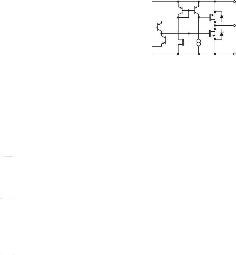
AMPLIFIER SECTION
The internal DACs output is buffered by a low power con-
sumption precision amplifier. The op amp has a 60 µs typical
settling time to 0.1% of full scale. There are slight differences in
settling time for negative slewing signals versus positive. Also,
negative transition settling time to within the last 6 LSBs of zero
volts has an extended settling time. The rail-to-rail output stage
of this amplifier has been designed to provide precision perfor-
mance while operating near either power supply. Figure 5
shows an equivalent output schematic of the rail-to-rail ampli-
fier with its N-channel pull-down FETs that will pull an output
load directly to GND. The output sourcing current is provided
by a P-channel pull-up device that can source current to GND
terminated loads.
AGND
V
OUT
V
DD
P-CH
N-CH
Figure 5. Equivalent Analog Output Circuit
The rail-to-rail output stage provides ±1 mA of output current.
The N-channel output pull-down MOSFET shown in Figure 5
has a 35 ON resistance, which sets the sink current capability
near ground. In addition to resistive load driving capability, the
amplifier has also been carefully designed and characterized for
up to 100 pF capacitive load driving capability.
REFERENCE INPUT
The reference input terminal has a constant input-resistance
independent of digital code which results in reduced glitches on
the external reference voltage source. The high 2 M input-
resistance minimizes power dissipation within the AD7390/
AD7391 D/A converters. The V
REF
input accepts input voltages
ranging from ground to the positive-supply voltage V
DD
. One of
the simplest applications which saves an external reference
voltage source is connection of the V
REF
terminal to the positive
V
DD
supply. This connection results in a rail-to-rail voltage
output span maximizing the programmed range. The reference
input will accept ac signals as long as they are kept within the
supply voltage range, 0 < V
REF IN
< V
DD
. The reference band-
width and integral nonlinearity error performance are plotted in
the typical performance section (see TPCs 14 and 15). The
ratiometric reference feature makes the AD7390/AD7391 an
ideal companion to ratiometric analog-to-digital converters such
as the AD7896.
POWER SUPPLY
The very low power consumption of the AD7390/AD7391 is a
direct result of a circuit design optimizing the use of a CBCMOS
process. By using the low power characteristics of CMOS for the
logic, and the low noise, tight-matching of the complementary
bipolar transistors, excellent analog accuracy is achieved. One
advantage of the rail-to-rail output amplifiers used in the AD7390/
AD7391 is the wide range of usable supply voltage. The part is
fully specified and tested for operation from 2.7 V to 5.5 V.
POWER SUPPLY BYPASSING AND GROUNDING
Precision analog products, such as the AD7390/AD7391, require
a well filtered power source. Since the AD7390/AD7391 operates
from a single 3 V to 5 V supply, it seems convenient to simply tap
into the digital logic power supply. Unfortunately, the logic sup-
ply is often a switch-mode design, which generates noise in the
20 kHz to 1 MHz range. In addition, fast logic gates can generate
glitches hundred of millivolts in amplitude due to wiring resis-
tance and inductance. The power supply noise generated thereby
means that special care must be taken to assure that the inherent
precision of the DAC is maintained. Good engineering judgment
should be exercised when addressing the power supply ground-
ing and bypassing of the AD7390.
REV. A
AD7390/AD7391
–9–
The AD7390 should be powered directly from the system
power supply. This arrangement, shown in Figure 6, employs an
LC filter and separate power and ground connections to isolate
the analog section from the logic switching transients.
FERRITE BEAD:
TWO TURNS, FAIR-RITE
#2677006301
TTL/CMOS
LOGIC
CIRCUITS
5V
POWER SUPPLY
100F
ELECT.
10F22F
TANTALUM
0.1F
CERAMIC
CAPACITOR
5V
5V
RETURN
Figure 6. Use Separate Traces to Reduce Power
Supply Noise
Whether or not a separate power supply trace is available, how-
ever, generous supply bypassing will reduce supply-line induced
errors. Local supply bypassing consisting of a 10 µF tantalum
electrolytic in parallel with a 0.1 µF ceramic capacitor is recom-
mended in all applications (Figure 7).
AD7390
OR
AD7391
0.1F
CLK
V
OUT
REF
V
DD
GND
C
*
10F
6
78
5
1
2
3
4
SDI
CLR
LD
*OPTIONAL EXTERNAL
REFERENCE BYPASS
2.7V TO 5.5V
Figure 7. Recommended Supply Bypassing
INPUT LOGIC LEVELS
All digital inputs are protected with a Zener-type ESD protection
structure (Figure 8) that allows logic input voltages to exceed the
V
DD
supply voltage. This feature can be useful if the user is driving
one or more of the digital inputs with a 5 V CMOS logic input-
voltage level while operating the AD7390/AD7391 on a 3 V power
supply. If this mode of interface is used, make sure that the V
OL
of the 5 V CMOS meets the V
IL
input requirement of the AD7390/
AD7391 operating at 3 V. See TPC 6 for a graph for digital
logic input threshold versus operating V
DD
supply voltage.
LOGIC
IN
V
DD
GND
Figure 8. Equivalent Digital Input ESD Protection
In order to minimize power dissipation from input-logic levels
that
are near the V
IH
and V
IL
logic input voltage specifications,
a
Schmitt trigger design was used that minimizes the input-buffer
current consumption compared to traditional CMOS input
stages. TPC 5 shows a plot of incremental input voltage versus
supply current showing that negligible current consumption
takes place when logic levels are in their quiescent state. The
normal crossover current still occurs during logic transitions. A
secondary advantage of this Schmitt trigger is the prevention of
false triggers that would occur with slow moving logic transi-
tions when a standard CMOS logic interface or opto isolators
are used. The logic inputs SDI, CLK, LD, CLR all contain the
Schmitt trigger circuits.
DIGITAL INTERFACE
The AD7390/AD7391 have a double-buffered serial data input.
The serial-input register is separate from the DAC register,
which allows preloading of a new data value into the serial regis-
ter without disturbing the present DAC values. A functional
block diagram of the digital section is shown in Figure 4, while
Table I contains the truth table for the control logic inputs.
Three pins control the serial data input. Data at the Serial Data
Input (SDI) is clocked into the shift register on the rising edge
of CLK. Data is entered in MSB-first format. Twelve clock
pulses are required to load the 12-bit AD7390 DAC value. If
additional bits are clocked into the shift register, for example
when a microcontroller sends two 8-bit bytes, the MSBs are
ignored (Figure 9). The CLK pin is only enabled when Load
(LD) is high. The lower resolution 10-bit AD7391 contains a
10-bit shift register. The AD7391 is also loaded MSB first with
10 bits of data. Again if additional bits are clocked into the shift
register, only the last 10 bits clocked in are used.
The Load pin (LD) controls the flow of data from the shift
register to the DAC register. After a new value is clocked into
the serial-input register, it will be transferred to the DAC register
by the negative transition of the Load pin (LD).
BYTE 1 BYTE 0
MSB LSB
MSB
LSB
B15 B14 B13 B12 B11 B10 B9 B8
B7 B6 B5 B4 B3 B2 B1 B0
X X X X D11 D10 D9 D8
D7 D6 D5 D4 D3 D2 D1 D0
X X X X X X D9 D8
D7 D6 D5 D4 D3 D2 D1 D0
D11D0: 12-BIT AD7390 DAC VALUE; D9D0: 10-BIT AD7391 DAC VALUE
X = DONT CARE
THE MSB OF BYTE 1 IS THE FIRST BIT THAT IS LOADED INTO THE DAC
Figure 9. Typical AD7390-Microprocessor Serial Data
Input Forms
RESET (CLR) PIN
Forcing the CLR pin low will set the DAC register to all zeros
and the DAC output voltage will be zero volts. The reset function
is useful for setting the DAC outputs to zero at power-up or
after a power supply interruption. Test systems and motor
controllers are two of many applications which benefit from
powering up to a known state. The external reset pulse can be
generated by the microprocessors power-on RESET signal, by
an output from the microprocessor, or by an external resistor
and capacitor. CLR has a Schmitt trigger input which results in
a clean reset function when using external resistor/capacitor
generated pulses. The CLR input overrides other logic inputs,
specifically LD. However, LD should be set high before CLR
goes high. If CLR is kept low, then the contents of the shift
register will be transferred to the DAC register as soon as CLR
returns high. See the Control-Logic Truth Table I.

AD7390ARZ-REEL7

Mfr. #:
Manufacturer:
Analog Devices Inc.
Description:
Digital to Analog Converters - DAC IC 12B +3V MICROPWR
Lifecycle:
New from this manufacturer.
Delivery:
DHL FedEx Ups TNT EMS
Payment:
T/T Paypal Visa MoneyGram Western Union