Data Sheet DAC08
Rev. D | Page 5 of 21
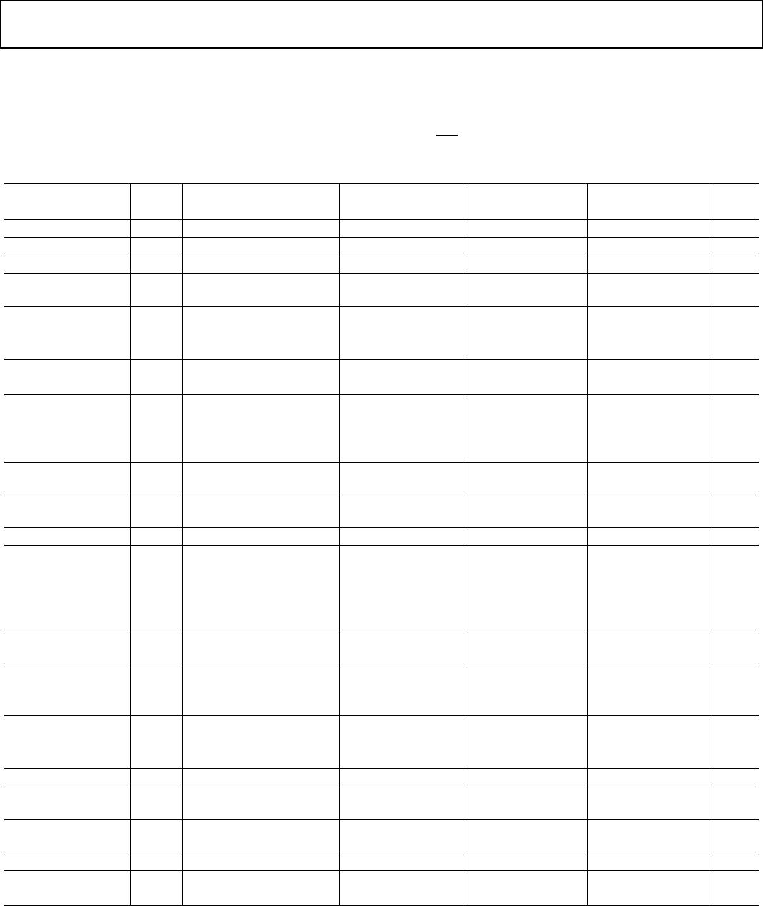
ABSOLUTE MAXIMUM RATINGS
Table 3.
Parameter Rating
Operating Temperature
DAC08AQ, DAC08Q −55°C to +125°C
DAC08HQ, DAC08EQ, DAC08CQ 0°C to +70°C
DAC08CP, DAC08CS −40°C to +85°C
Junction Temperature (T
J
) −65°C to +150°C
Storage Temperature Q Package −65°C to +150°C
Storage Temperature P Package −65°C to +125°C
Lead Temperature (Soldering, 60 sec) 300°C
V+ Supply to V− Supply 36 V
Logic Inputs V− to V− + 36 V
V
LC
V− to V+
Analog Current Outputs (at V
S−
= 15 V) 4.25 mA
Reference Input (V
14
to V
15
) V− to V+
Reference Input Differential Voltage
(V
14
to V
15
) ±18 V
Reference Input Current (I
14
) 5.0 mA
Stresses at or above those listed under Absolute Maximum
Ratings may cause permanent damage to the product. This is a
stress rating only; functional operation of the product at these
or any other conditions above those indicated in the operational
section of this specification is not implied. Operation beyond
the maximum operating conditions for extended periods may
affect product reliability.
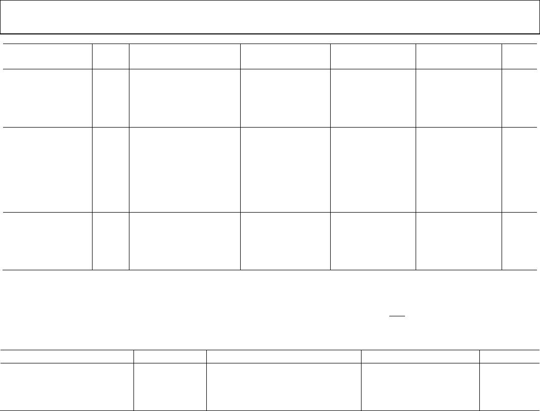
THERMAL RESISTANCE
θ
JA
is specified for worst case mounting conditions, that is, θ
JA
is
specified for device in socket for CERDIP, PDIP, and LCC
packages; θ
JA
is specified for device soldered to printed circuit
board for SOIC package.
Table 4. Thermal Resistance
Package Type θ
JA
θ
JC
Unit
16-Lead CERDIP (Q) 100 16 °C/W
16-Lead PDIP (P) 82 39 °C/W
20-Terminal LCC (RC) 76 36 °C/W
16-Lead SOIC (S) 111 35 °C/W
ESD CAUTION