8
Notes:
1. Bypassing the power supply line is required with a 0.1 µF ceramic
disc capacitor adjacent to each optocoupler as illustrated in Figure
19. The power supply bus for the optocoupler(s) should be separate
from the bus for any active loads, otherwise a larger value of bypass
capacitor (up to 0.5 µF) may be needed to suppress regenerative
feedback via the power supply.
2. Peaking circuits may produce transient input currents up to 100
mA, 500 ns maximum pulse width, provided average current does
not exceed 5 mA.
3. Device considered a two terminal device: pins 1, 2, 3, and 4 shorted
together, and pins 5, 6, 7, and 8 shorted together.
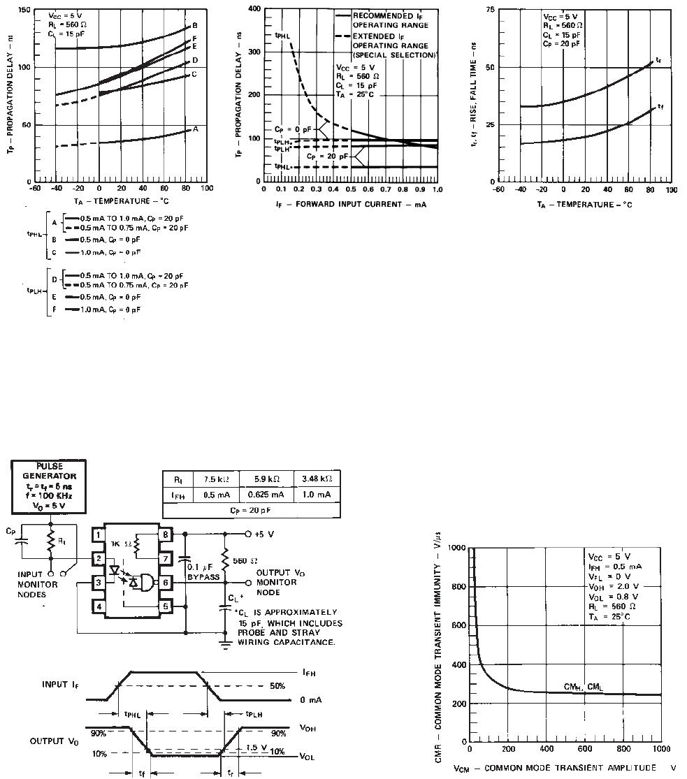
4. The t
PLH
propagation delay is measured from the 50% point on the
trailing edge of the input pulse to the 1.5 V point on the trailing
edge of the output pulse.
5. The t
PHL
propagation delay is measured from the 50% point on the
leading edge of the input pulse to the 1.5 V point on the leading
edge of the output pulse.
6. CM
H
is the maximum tolerable rate of rise of the common mode
voltage to assure that the output will remain in a high logic state
(i.e., V
OUT
> 2.0 V).
7. CM
L
is the maximum tolerable rate of fall of the common mode
voltage to assure that the output will remain in a low logic state
(i.e., V
OUT
< 0.8 V).
8. C
P
is the peaking capacitance. Refer to test circuit in Figure 8.
9. In accordance with UL 1577, each optocoupler is momentary with-
stand proof tested by applying an insulation test voltage ≥4500
Vrms for 1 second (leakage detection current limit, I
I-O
≤ 5 µA). This
test is performed before the 100% production test for partial dis-
charge (Method b) shown in the IEC/EN/DIN EN 60747-5-5 Insula-
tion Character istics Table, if applicable.
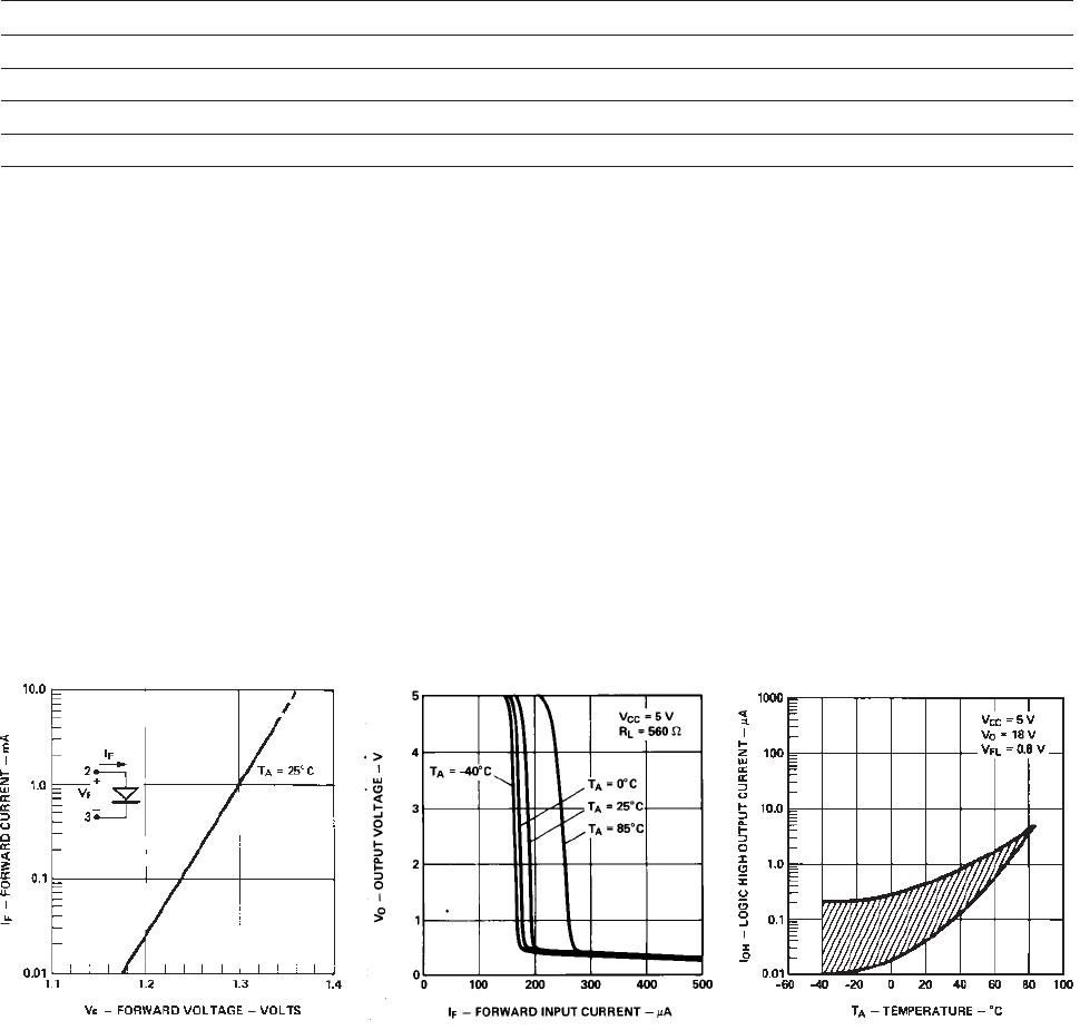
Figure 3. Typical output voltage vs. forward
input current vs. temperature.
Figure 2. Typical input diode forward charac-
teristics.
Figure 4. Typical logic high output current vs.
temperature.
Package Characteristics
For -40°C ≤T
A
≤85°C, unless otherwise specied. All typicals at T
A
= 25°C.
Parameter Symbol Min. Typ. Max. Units Test Conditions Fig. Notes
Input-Output Momentary V
ISO
3750 V
rms
RH ≤ 50%, t = 1 min, 3, 9
Withstand Voltage* T
A
= 25°C
Resistance, Input-Output R
I-O
1012 Ω V
I-O
= 500 V 3
Capacitance, Input-Output C
I-O
0.6 pF f = 1 MHz 3
*The Input-Output Momentary Withstand Voltage is a dielectric voltage rating that should not be interpreted as an input-output continuous voltage
rating. For the continuous voltage rating refer to the IEC/EN/DIN EN 60747-5-5 Insulation Characteristics Table (if applicable), your equipment level
safety specication, or Avago Application Note 1074, “Optocoupler Input-Output Endurance Voltage.”