NCN4555
http://onsemi.com
3
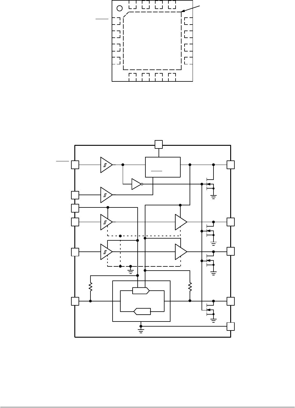
PIN DESCRIPTIONS
PIN Name Type Description
1 STOP INPUT Power Down Mode pin:
STOP = Low ³ Low current shutdown mode activated
STOP = High ³ Normal Operation
A Low level on this pin resets the SIM interface, switching off the SIM_V
CC
.
2 MOD_V
CC
INPUT The signal present on this pin programs the SIM_V
CC
value:
MOD_V
CC
= Low ³ SIM_V
CC
= 1.8 V
MOD_V
CC
= High ³ SIM_V
CC
= 3 V
3 V
DD
POWER This pin is connected to the system controller power supply. It configures the level shifter input
stage to accept the signals coming from the microprocessor. A 0.1 mF capacitor shall be used to
bypass the power supply voltage. When V
DD
is below 1.1 V typical the SIM_V
CC
is disabled. The
NCN4555 comes into a shutdown mode.
4 NC No Connect
5 V
BAT
POWER DC−DC converter supply input. The input voltage ranges from 2.7V up to 5.5V. This pin has to be
bypass by a 0.1 mF capacitor.
6 NC No Connect
7 SIM_V
CC
POWER This pin is connected to the SIM card power supply pin. An internal LDO converter is
programmable by the external MPU to supply either 1.8 V or 3.0 V output voltage. An external
1.0 mF minimum ceramic capacitor recommended must be connected across SIM_V
CC
and GND.
During a normal operation, the SIM_V
CC
voltage can be set to 1.8 V followed by a 3.0 V value, or
can start directly to any of these two values.
8 SIM_I/O INPUT/
OUTPUT
This pin handles the connection to the serial I/O of the card connector. A bidirectional level
translator adapts the serial I/O signal between the card and the micro controller. A 14 kW (typical)
pullup resistor provides a High impedance state for the SIM card I/O link.
9 SIM_RST OUTPUT This pin is connected to the RESET pin of the card connector. A level translator adapts the
external Reset (RST) signal to the SIM card.
10 GND GROUND This pin is the GROUND reference for the integrated circuit and associated signals. Care must be
taken to avoid voltage spikes when the device operates in a normal operation.
11 SIM_CLK OUTPUT This pin is connected to the CLOCK pin of the card connector. The CLOCK (CLK) signal comes
from the external clock generator, the internal level shifter being used to adapt the voltage defined
for the SIM_V
CC
.
12 NC No Connect
13 CLK INPUT The clock signal, coming from the external controller, must have a Duty Cycle within the Min/Max
values defined by the specification (typically 50%). The built−in level shifter translates the input
signal to the external SIM card CLK input.
14 RST INPUT The RESET signal present at this pin is connected to the SIM card through the internal level
shifter which translates the level according to the SIM_V
CC
programmed value.
15 I/O INPUT/
OUTPUT
This pin is connected to an external microcontroller or cellular phone management unit. A
bidirectional level translator adapts the serial I/O signal between the smart card and the external
controller. A built−in constant 18 kW (typical) resistor provides a high impedance state when not
activated.
16 NC No Connect