NCN4555
http://onsemi.com
5
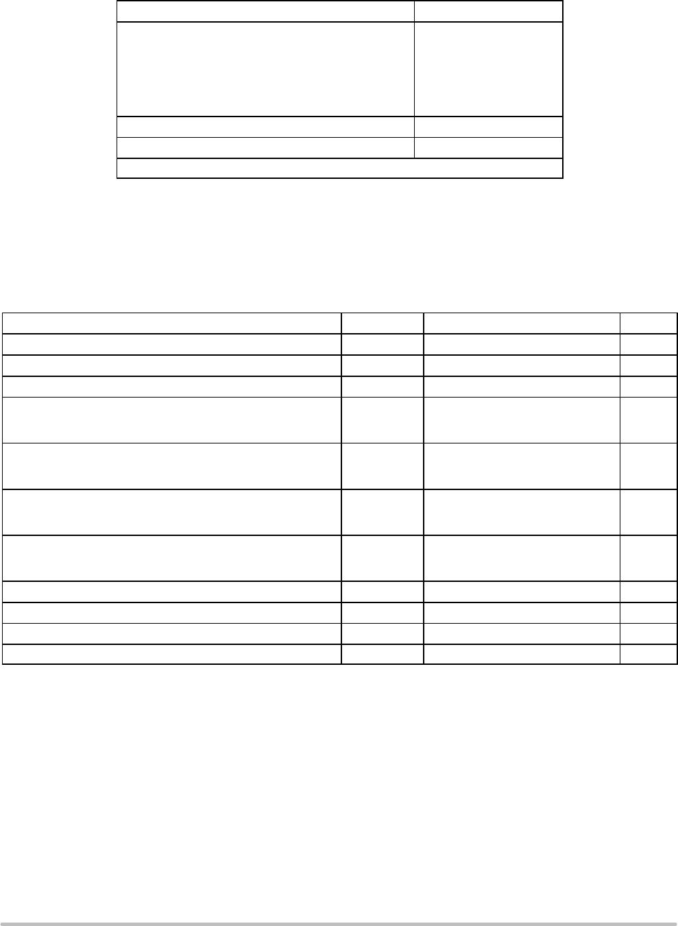
POWER SUPPLY SECTION (−25°C to +85°C)
Pin Symbol Rating Min Typ Max Unit
5 V
BAT
Power Supply 2.7 5.5 V
5 I
VBAT
Operating current – I
CC
= 0 mA (Note 6) 22 30
mA
5 I
VBAT_SD
Shutdown current – STOP= Low (Note 7) 3.0
mA
3 V
DD
Operating Voltage 1.8 5.5 V
3 I
VDD
Operating Current – f
CLK
= 1 MHz (Note 8) 7.0 12
mA
3 I
VDD_SD
Shutdown Current – STOP = Low 1.0
mA
3 V
DD
Undervoltage Lockout 0.6 1.5 V
7 SIM_V
CC
MOD_V
CC
= High, V
BAT
= 3.0 V, I
SIM_VCC
= 50 mA
MOD_V
CC
= High, V
BAT
= 3.3 V to 5.5 V, I
SIM_VCC
= 0 mA to 50 mA
MOD_V
CC
= Low, V
BAT
= 2.7 V to 5.5 V, I
SIM_VCC
= 0 mA to 50 mA
2.8
1.7
2.8
3.0
1.8
3.2
1.9
V
V
V
7 I
SIM_VCC_SC
Short –Circuit Current – SIM_V
CC
shorted to ground , T
A
=25°C 175 mA
NOTE: Device will meet the specifications after thermal equilibrium has been established when mounted in a test socket or printed circuit
board with maintained transverse airflow greater than 500 lfpm. Electrical parameters are guaranteed only over the declared
operating temperature range. Functional operation of the device exceeding these conditions is not implied. Device specification limit
values are applied individually under normal operating conditions and not valid simultaneously.
6. As long as V
BAT
– V
DD
v
2.5 V. For V
BAT
– V
DD
> 2.5 V the maximum value increases up to 35 mA (typical being in the +25 mA range).
7. As long as V
BAT
– V
DD
v
2.5 V.
8. Guaranteed by design over the operating temperature range specified.
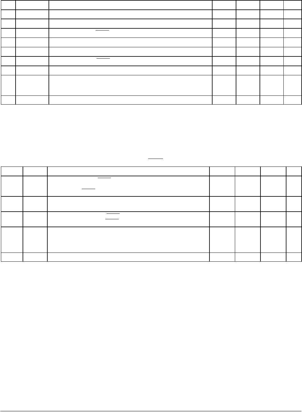
DIGITAL INPUT/OUTPUT SECTION CLOCK, RESET, I/O, STOP, MOD_V
CC
Pin Symbol Rating Min Typ Max Unit
1,2, 13,
14, 15
V
in
I
IH
& I
IL
Input Voltage Range (STOP, MOD_V
CC
, RST, CLK, I/O)
Input Current (STOP, MOD_V
CC
, RST, CLK)
0
−100
V
DD
100
V
nA
13, 14 V
IH
V
IL
High Level Input Voltage (RST, CLK)
Low Level Input Voltage (RST, CLK)
0.7 * V
DD
V
DD
0.2 * V
DD
V
V
1, 2 V
IH
V
IL
High Level Input Voltage (STOP, MOD_V
CC
)
Low Level Input Voltage (STOP, MOD_V
CC
)
0.7 * V
DD
0
V
DD
0.4
V
V
15 V
OH_I/O
V
OL_I/O
I
IH
I
IL
High Level Output Voltage (SIM_I/O = SIM_V
CC
, I
OH_I/O
= −20 mA)
Low Level Output Voltage (SIM_I/O = 0 V, I
OH_I/O
= 200 mA)
High Level Input Current (I/O)
Low Level Input Current (I/O)
0.7 * V
DD
0
−20
V
DD
0.4
20
1.0
V
V
mA
mA
15 R
pu_I/O
I/0 Pullup Resistor 12 18 24
kW
NOTE: Device will meet the specifications after thermal equilibrium has been established when mounted in a test socket or printed circuit
board with maintained transverse airflow greater than 500 lfpm. Electrical parameters are guaranteed only over the declared
operating temperature range. Functional operation of the device exceeding these conditions is not implied. Device specification limit
values are applied individually under normal operating conditions and not valid simultaneously.