NCN4555
http://onsemi.com
7
TYPICAL CHARACTERISTICS
50
60
70
80
90
100
−50 −30 −10 10 30 50 70 90
TEMPERATURE (°C)
IVCC_SC_1.8 V (mA)
V
BAT
= 2.7 V
V
BAT
= 5.5 V
Figure 4. Short Circuit Current IV
CC
_SC vs
Temperature at SIM_V
CC
= 1.8 V (MOD_V
CC
= LOW)
10
15
20
25
30
−50 −30 −10 10 30 50 70 90
TEMPERATURE (°C)
IVCC_SC_3.0 V (
m
A)
V
BAT
= 3.3 V
V
BAT
= 5.5 V
50
60
70
80
90
100
−50 −30 −10 10 30 50 70 9
0
V
BAT
= 3.3 V
V
BAT
= 5.5 V
TEMPERATURE (°C)
IVCC_SC_3.0 V (mA)
Figure 5. Short Circuit Current IV
CC
_SC vs
Temperature at SIM_V
CC
= 3.0 V (MOD_V
CC
= HIGH
)
Figure 6. I
BAT
vs temperature at 3.0 V
10
15
20
25
30
−50 −30 −10 10 30 50 70 9
0
V
BAT
= 2.7 V
V
BAT
= 5.5 V
TEMPERATURE (°C)
IVCC_SC_1.8 V (mA)
Figure 7. IV
BAT
vs Temperature at 1.8 V
NCN4555
http://onsemi.com
8
APPLICATION INFORMATION
CARD SUPPLY CONVERTER
The NCN4555 interface DC−DC converter is a
Low Dropout Voltage Regulator capable of suppling a
current in excess of 50 mA under 1.8 V or 3.0 V. This device
features a very low quiescent current typically lower than
25 mA (Figure 6 and 7). MOD_V
CC
is a select input
allowing a logic level signal to select a regulated voltage of
1.8 V (MOD_V
CC
= LOW) or 3.0 V (MOD_V
CC
= HIGH).
Additionally, the NCN4555 has a shutdown input allowing
it to turn off or turn on the regulator output. The shutdown
mode power consumption is typically in the range of a few
tens of nA (30 nA Typical). Figure 8 shows a simplified
view of the NCN4555 voltage regulator. The SIM_V
CC
output is internally current limited and protected against
short circuits. The short−circuit current IV
CC
is constant
over the temperature and SIM_V
CC
. It varies with V
BAT
typically in the range of 60 mA to 90 mA (Figure 4 and 5).
In order to guarantee a stable and satisfying operating of
the LDO the SIM_V
CC
output will be connected to a 1.0 mF
bypass ceramic capacitor to the ground. At the input, V
BAT
will be bypassed to the ground with a 0.1 mF ceramic
capacitor.
LEVEL SHIFTERS
The level shifters accommodate the voltage difference
that might exist between the microcontroller and the smart
card. The RESET and CLOCK level shifters are
monodirectional and feature both the same architecture.
The bidirectional I/O line provides a way to automatically
adapt the voltage difference between the MCU and the SIM
card in both directions. In addition with the pullup resistor,
an active pullup circuit (Figure 8, Q1 and Q2) provides a fast
charge of the stray capacitance, yielding a rise time fully
within the ISO7816 specifications.
+
Figure 8. Simplified Block Diagram of the LDO Voltage Regulator
+
R1
R2
GND
Q1
V
REF
C
IN
= 0.1 mF
V
BAT
STOP
SIM_V
CC
MOD_V
CC
C
OUT
= 1.0 mF
I
lim
Figure 9. Basic I/O Line Interface
LOGICIO/CONTROL
GND
GND
Q3
SIM_I/OI/O
200 ns200 ns
Q2
Q1
18 k 14 k
V
DD
SIM_V
CC
NCN4555
http://onsemi.com
9
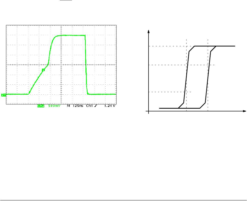
The typical waveform provided in Figure 10 shows how
the accelerator operates. During the first 200 ns (typical),
the slope of the rise time is solely a function of the pullup
resistor associated with the stray capacitance. During this
period, the PMOS devices are not activated since the input
voltage is below their V
gs
threshold. When the input slope
crosses the V
gsth
, the opposite one shot is activated,
providing a low impedance to charge the capacitance, thus
increasing the rise time as depicted in Figure 10. The same
mechanism applies for the opposite side of the line to make
sure the system is optimum.
INPUT SCHMITT TRIGGERS
All the Logic input pins (excepted I/O and SIM_I/O, See
Figure 3) have built−in Schmitt trigger circuits to prevent
the NCN4555 against uncontrolled operation. The typical
dynamic characteristics of the related pins are depicted
Figure 11.
The output signal is guaranteed to go High when the input
voltage is above 0.7 x V
DD
, and will go Low when the input
voltage is below 0.2 x V
DD
or 0.4 V depending on the input
considered (see the Digital Input Table on page 5).
SHUTDOWN OPERATING
In order to save power or for other purpose required by the
application it is possible to put the NCN4555 in a shutdown
mode by setting Low the pin STOP. On the other hand the
device enters automatically in a shutdown mode when V
DD
becomes lower than 1.1 V typically.
ESD PROTECTION
The NCN4555 SIM interface features an HBM ESD
voltage protection in excess of 7 kV for all the SIM pins
(SIM_IO, SIM_CLK, SIM_RST, SIM_V
CC
and GND). All
the other pins (microcontroller side) sustain at least 2 kV.
These values are guaranteed for the device in its full integrity
without considering the external capacitors added to the
circuit for a proper operating. Consequently in the operating
conditions it is able to sustain much more than 7 kV on its
SIM pins making it perfectly protected against electrostatic
discharge well over the HBM ESD voltages required by the
ISO7816 standard (4 kV).
PRINTED CIRCUIT BOARD LAYOUT
Careful layout routing will be applied to achieve a good
and efficient operating of the device in its mobile or portable
environment and fully exploit its performance.
The bypass capacitors have to be connected as close as
possible to the device pins (SIM_V
CC
, V
DD
or V
BAT
) in
order to reduce as much as possible parasitic behaviors
(ripple and noise). It is recommended to use
ceramic capacitors.
The exposed pad of the QFN−16 package will be
connected to the ground as well as the unconnected pins
(NC). A relatively large ground plane is recommended.
Figures 12 and 13 shows an example of PCB device
implementation in an evaluation environment.
Figure 10. SIM_IO Typical Rise and Fall Times with
Stray Capacitance > 30 pF
(33 pF Capacitor Connected on the Board)
OUTPUT
V
DD
ON
OFF
0.2 x V
DD
or 0.4 V
0.7 x V
DD
INPUT
Figure 11. Typical Schmitt Trigger Characteristics

NCN4555MNR2

Mfr. #:
Manufacturer:
ON Semiconductor
Description:
IC TRNSLTR BIDIRECTIONAL 16QFN
Lifecycle:
New from this manufacturer.
Delivery:
DHL FedEx Ups TNT EMS
Payment:
T/T Paypal Visa MoneyGram Western Union

Products related to this Datasheet