10
LTC3401
3401fb
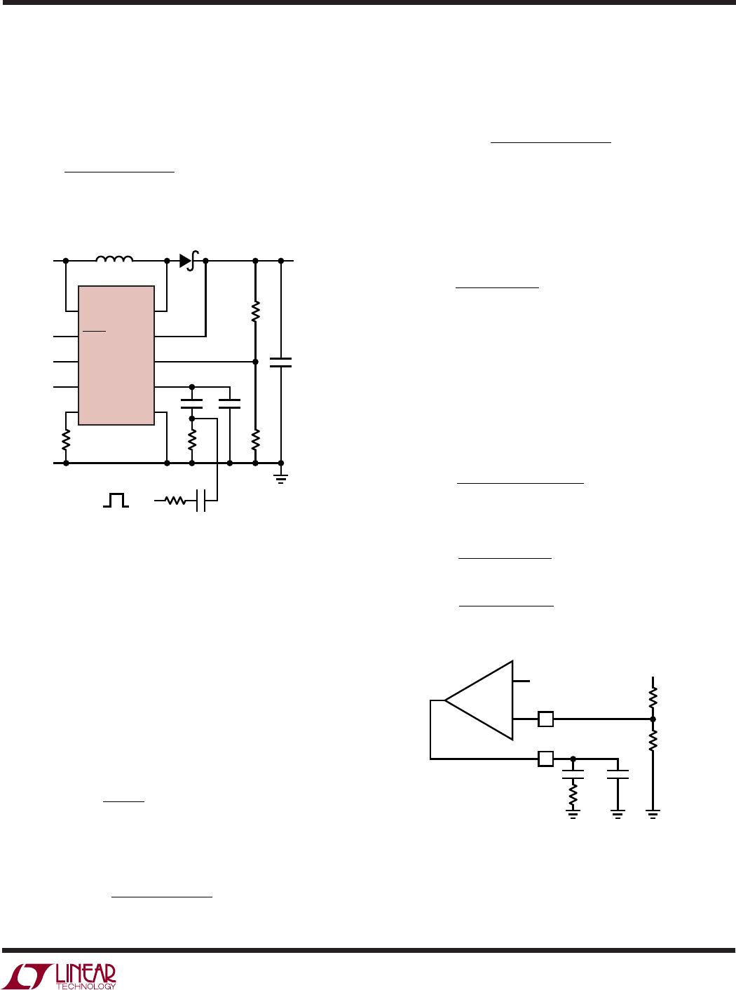
In some layouts it may be required to place a 1μF low ESR
capacitor as close to the V
OUT
and GND pins as possible.
Input Capacitor Selection
The input filter capacitor reduces peak currents drawn from
the input source and reduces input switching noise. Since
the IC can operate at voltages below 0.5V once the output
is regulated, demand on the input capacitor is much less
and in most applications a 3.3μF is sufficient.
Output Diode
For applications with output voltages over 4.3V, a Schottky
diode is required to ensure that the SW pin voltage does
not exceed its absolute maximum rating. The Schottky
diode across the synchronous PMOS switch provides a
lower drop during the break-before-make time (typically
20ns) of the NMOS to PMOS transition. The Schottky
diode improves peak efficiency (see graph “Efficiency
Loss Without Schottky vs Frequency”). Use of a Schottky
diode such as a MBRM120T3, 1N5817 or equivalent.
Since slow recovery times will compromise efficiency, do
not use ordinary rectifier diodes.
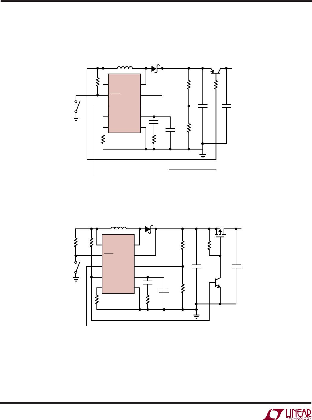
Operating Frequency Selection
There are several considerations in selecting the operat-
ing frequency of the converter. The first is determining
the sensitive frequency bands that cannot tolerate any
spectral noise. For example, in products incorporating
RF communications, the 455kHz IF frequency is sensitive
to any noise, therefore switching above 600kHz is de-
sired. Some communications have sensitivity to 1.1MHz.
APPLICATIO S I FOR ATIO
WUUU
In this case, converter frequencies up to 3MHz may be
employed.
The second consideration is the physical size of the
converter. As the operating frequency goes up, the induc-
tor and filter caps go down in value and size. The trade off
is in efficiency since the switching losses due to gate
charge are going up proportional with frequency. For
example in Figure 2, for a 2.4V to 3.3V converter, the
efficiency at 100mA is 5% less at 2MHz compared to
300kHz.
Another operating frequency consideration is whether the
application can allow “pulse skipping.” In this mode, the
minimum on time of the converter cannot support the duty
cycle, so the converter ripple will go up and there will be
a low frequency component of the output ripple. In many
applications where physical size is the main criterion then
running the converter in this mode is acceptable. In
applications where it is preferred not to enter this mode,
then the maximum operating frequency is given by:
f
VV
Vt
Hz
MAX NOSKIP
OUT IN
OUT ON MIN
_
()
–
•
=
where t
ON(MIN)
= minimum on time = 120ns
Reducing Output Capacitance with a Load Feed
Forward Signal
In many applications the output filter capacitance can be
reduced for the desired transient response by having the
device commanding the change in load current, (i.e.
system microcontroller), inform the power converter of
the changes as they occur. Specifically, a “load feed
forward” signal coupled into the V
C
pin gives the inner
current loop a head start in providing the change in output
current. The transconductance of the LTC3401 converter
at the V
C
pin with respect to the inductor current is typically
130mA/100mV, so the amount of signal injected is pro-
portional to the anticipated change of inductor current
with load. The outer voltage loop performs the remainder
of the correction, but because of the load feed forward
signal, the range over which it must slew is greatly
reduced. This results in an improved transient response.
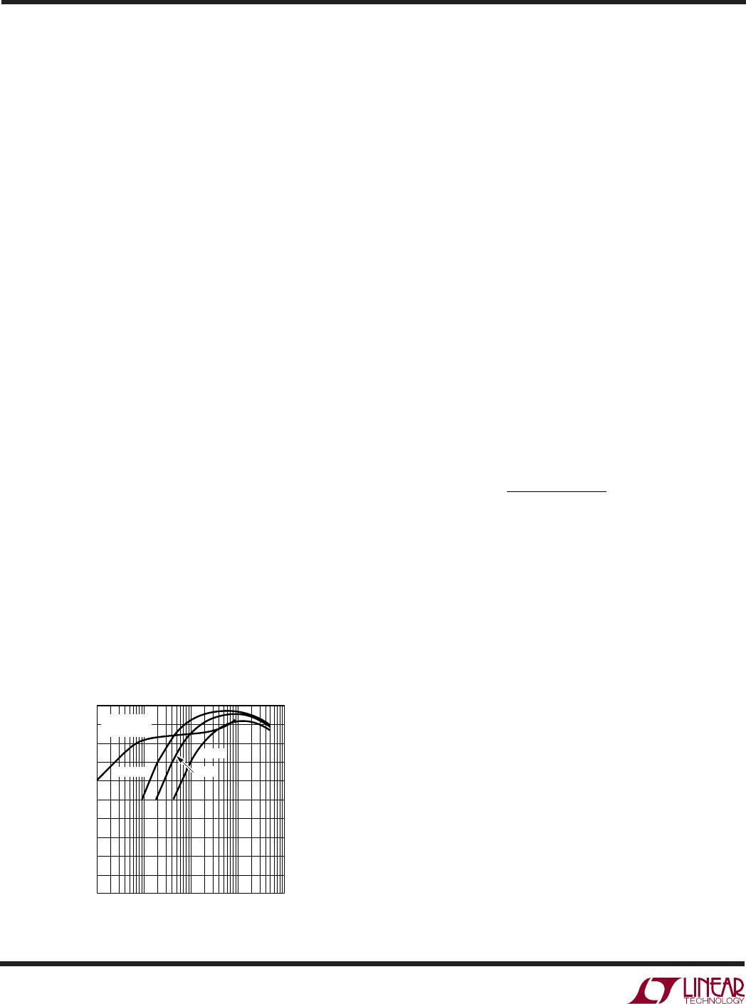
Figure 2. Converter Efficiency 2.4V to 3.3V
OUTPUT CURRENT (mA)
30
EFFICIENCY (%)
90
100
20
10
80
50
70
60
40
0.1 10 100 1000
3401 G08
0
1
300kHz
3MHz
1MHz
Burst Mode
OPERATION