4
LTC3401
3401fb
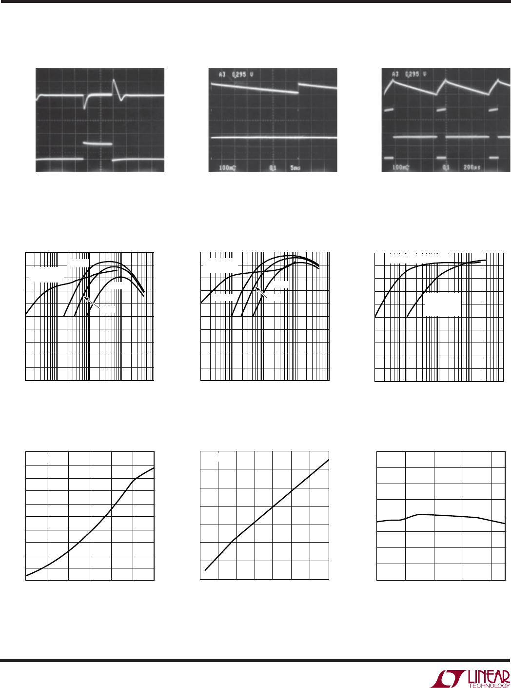
Transient Response 50mA to 500mA
TYPICAL PERFOR A CE CHARACTERISTICS
UW
Burst Mode Operation
V
OUT
200mV/DIV
550mA
50mA
I
OUT
C
OUT
= 22μF 200μs/DIV 3401 G04
L = 3.3μH
f
OSC
= 1MHz
V
OUT
AC
100mV/DIV
V
IN
= 1.2V 5ms/DIV 3401 G05
V
OUT
= 3.3V
C
OUT
= 100μF
I
OUT
= 250μA
MODE/SYNC PIN = HIGH
SW
1V/DIV
V
OUT
AC
100mV/DIV
V
IN
= 1.2V 200μs/DIV 3401 G06
V
OUT
= 3.3V
C
OUT
= 100μF
I
OUT
= 20mA
MODE/SYNC PIN = HIGH
SW
1V/DIV
Converter Efficiency 1.2V to 3.3V
OUTPUT CURRENT (mA)
EFFICIENCY (%)
80
100
60
0
40
20
70
90
50
30
10
0.1 10 100 1000
3401 G07
1
Burst Mode
OPERATION
3MHz
300kHz
1MHz
OUTPUT CURRENT (mA)
30
EFFICIENCY (%)
90
100
20
10
80
50
70
60
40
0.1 10 100 1000
3401 G08
0
1
300kHz
3MHz
1MHz
Burst Mode
OPERATION
V
IN
(V)
0.8
0
OUTPUT CURRENT (mA)
100
200
300
0.9
1
1.1 1.2
3401 G09
1.3
400
500
1.4
T
A
= 25°C
Converter Efficiency 2.4V to 3.3V
Start-Up Voltage
vs I
OUT
LOAD CURRENT (mA)
0.1
0
EFFICIENCY (%)
10
30
40
50
100
70
3401 G10
20
80
90
60
110
100
1000
1MHz
FIXED
FREQUENCY
Burst Mode OPERATION
Converter Efficiency 3.6V to 5V
Efficiency Loss Without Schottky
vs Frequency
FREQUENCY (MHz)
0.2
8
10
14
1.4 2.2
3401 G11
6
4
0.6 1.0
1.8 2.6 3.0
2
0
12
EFFICIENCY LOSS (%)
T
A
= 25°C
Current Limit
TEMPERATURE (°C)
–55
CURRENT (A)
1.55
1.60
1.65
65
125
3401 G12
1.50
1.45
1.40
–15 25 105
1.70
1.75
1.80
5
LTC3401
3401fb
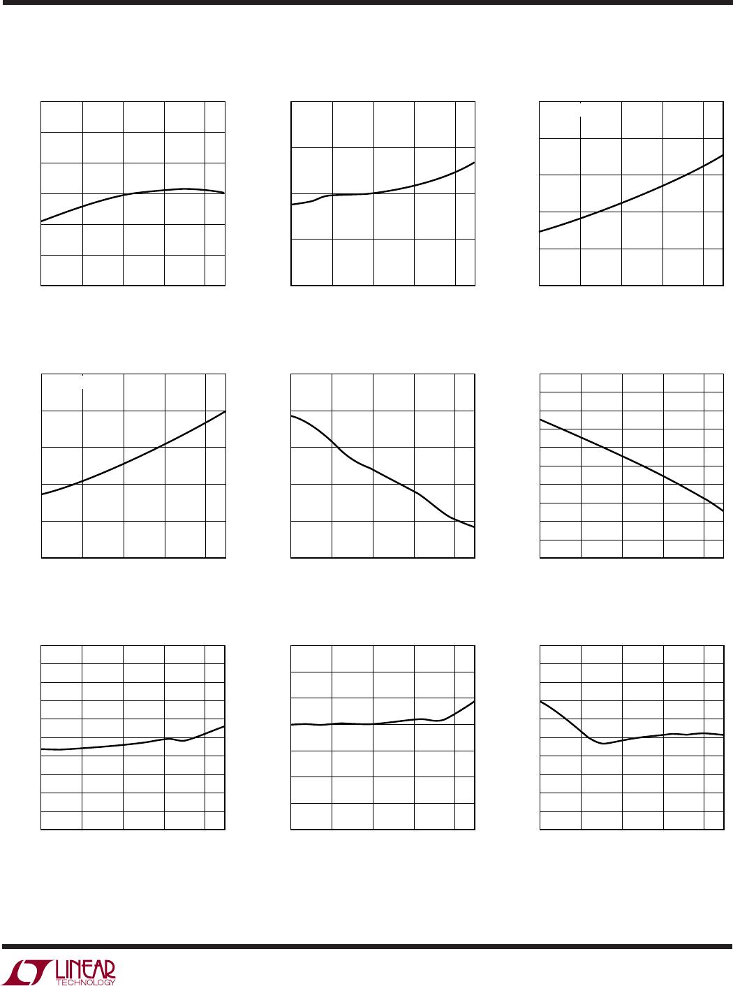
EA FB Voltage
TYPICAL PERFOR A CE CHARACTERISTICS
UW
Oscillator Frequency Accuracy
TEMPERATURE (°C)
–55
VOLTAGE (V)
1.23
1.24
1.25
65
125
3401 G13
1.22
–15 25 105
1.26
1.27
1.28
TEMPERATURE (°C)
–55
FREQUENCY (MHz)
2.00
65
125
3401 G14
1.95
1.90
–15 25 105
2.05
2.10
R
t
= 15k
PMOS R
DS(ON)
Start-Up Voltage
Shutdown Threshold
TEMPERATURE (°C)
–55
RESISTANCE (Ω)
0.15
65
125
3401 G16
0.10
0.05
–15 25 105
0.20
0.25
0.30
V
OUT
= 3.3V
TEMPERATURE (°C)
–55
VOLTAGE (V)
0.8
65
125
3401 G17
0.7
0.6
–15 25 105
0.9
1.0
1.1
TEMPERATURE (°C)
–55
VOLTAGE (V)
0.80
65
125
3401 G18
0.70
0.60
–15 25 105
0.90
1.00
1.10
0.75
0.65
0.85
0.95
1.05
PGOOD Threshold
Burst Mode Operation Current
V
OUT
Turn-Off Voltage
TEMPERATURE (°C)
–55
PERCENT FROM V
FB
(%)
10.0
65
125
3401 G19
11.0
12.0
–15 25 105
9.0
8.0
7.0
10.5
11.5
9.5
8.5
7.5
TEMPERATURE (°C)
–55
CURRENT (μA)
36
38
65
125
3401 G20
34
32
30
–15 25 105
40
42
44
TEMPERATURE (°C)
–55
VOLTAGE (V)
2.20
65
125
3401 G21
2.10
2.00
–15 25 105
2.30
2.40
2.50
2.15
2.05
2.25
2.35
2.45
NMOS R
DS(ON)
TEMPERATURE (°C)
–55
RESISTANCE (Ω)
0.15
65
125
3401 G22
0.10
0.05
–15 25 105
0.20
0.25
0.30
V
OUT
= 3.3V
6
LTC3401
3401fb
R
t
(Pin 1): Timing Resistor to Program the Oscillator
Frequency.
f
R
Hz
OSC
t
=
310
10
MODE/SYNC (Pin 2): Burst Mode Select and Oscillator
Synchronization.
MODE/SYNC = High. Enable Burst Mode operation. The
inductor peak inductor current will be 1/3 the current
limit value and return to zero current on each cycle.
During Burst Mode operation the operation is variable
frequency, providing a significant efficiency improve-
ment at light loads. It is recommended the Burst Mode
operation only be entered once the part has started up.
MODE/SYNC = Low. Disable Burst Mode operation and
maintain low noise, constant frequency operation.
MODE/SYNC = External CLK. Synchronization of the
internal oscillator and Burst Mode operation disable. A
clock pulse width of 100ns to 2μs is required to
synchronize.
V
IN
(Pin 3): Input Supply Pin.
SW (Pin 4): Switch Pin. Connect inductor and Schottky
diode here. For applications with output voltages over
4.3V, a Schottky diode is required to ensure that the SW
pin voltage does not exceed its absolute maximum rating.
Minimize trace length to keep EMI down. For discontinu-
ous inductor current, a controlled impedance is placed
UU
U
PI FU CTIO S
from SW to V
IN
from the IC to eliminate high frequency
ringing due to the resonant tank of the inductor and SW
node capacitance, therefore reducing EMI radiation.
GND (Pin 5): Signal and Power Ground for the IC.
PGOOD (Pin 6): Power Good Comparator Output. This
open-drain output is low when V
FB
< –9% from its
regulation voltage.
V
OUT
(Pin 7): Output of the Synchronous Rectifier and
Bootstrapped Power Source for the IC. A ceramic capaci-
tor of at least 1μF is required and should be located as
close to the V
OUT
and GND pins as possible (Pins 7 and 5).
FB (Pin 8): Feedback Pin. Connect resistor divider tap
here. The output voltage can be adjusted from 2.6V to
5.5V. The feedback reference voltage is typically 1.25V.
V
C
(Pin 9): Error Amp Output. A frequency compensation
network is connected to this pin to compensate the loop.
See the section “Compensating the Feedback Loop” for
guidelines.
SHDN (Pin 10): Shutdown. Grounding this pin shuts down
the IC. Tie to >1V to enable (V
IN
or digital gate output). To
operate with input voltages below 1V once the converter
has started, a 1M resistor from SHDN to V
IN
, and a 5M
resistor from SHDN to V
OUT
will provide sufficient hyster-
esis During shutdown the output voltage will hold up to V
IN
minus a diode drop due to the body diode of the PMOS
synchronous switch. If the application requires a com-
plete disconnect during shutdown then refer to section
“Output Disconnect Circuits”.
LTC3401EMS#PBF

Mfr. #:
Manufacturer:
Analog Devices / Linear Technology
Description:
Switching Voltage Regulators 1A, 3MHz uP Sync Boost Conv
Lifecycle:
New from this manufacturer.
Delivery:
DHL FedEx Ups TNT EMS
Payment:
T/T Paypal Visa MoneyGram Western Union

Products related to this Datasheet