2005-2013 Microchip Technology Inc. DS21939B-page 1
TC4426AM/TC4427AM/TC4428AM
Features
• High Peak Output Current: 1.5A
• Wide Input Supply Voltage Operating Range:
- 4.5V to 18V
• High Capacitive Load Drive Capability:
- 1000 pF in 25 ns (typ.)
• Short Delay Times: 30 ns (typ.)
• Matched Rise, Fall and Delay Times
• Low Supply Current:
- With Logic ‘1’ Input – 1 mA (typ.)
- With Logic ‘0’ Input – 100 µA (typ.)
• Low Output Impedance: 7(typ.)
• Latch-Up Protected: Will Withstand 0.5A Reverse
Current
• Input: Will Withstand Negative Inputs Up to 5V
• ESD Protected: 4 kV
• Pin-compatible with the
TC426M/TC427M/TC428M and
TC4426M/TC4427M/TC4428M
• Wide Operating Temperature Range:
- -55°C to +125°C
• See TC4426A/TC4427A/TC4428A Data Sheet
(DS21423) for additional temperature range and
packaging offerings
Applications
• Switch-mode Power Supplies
• Line Drivers
• Pulse Transformer Drive
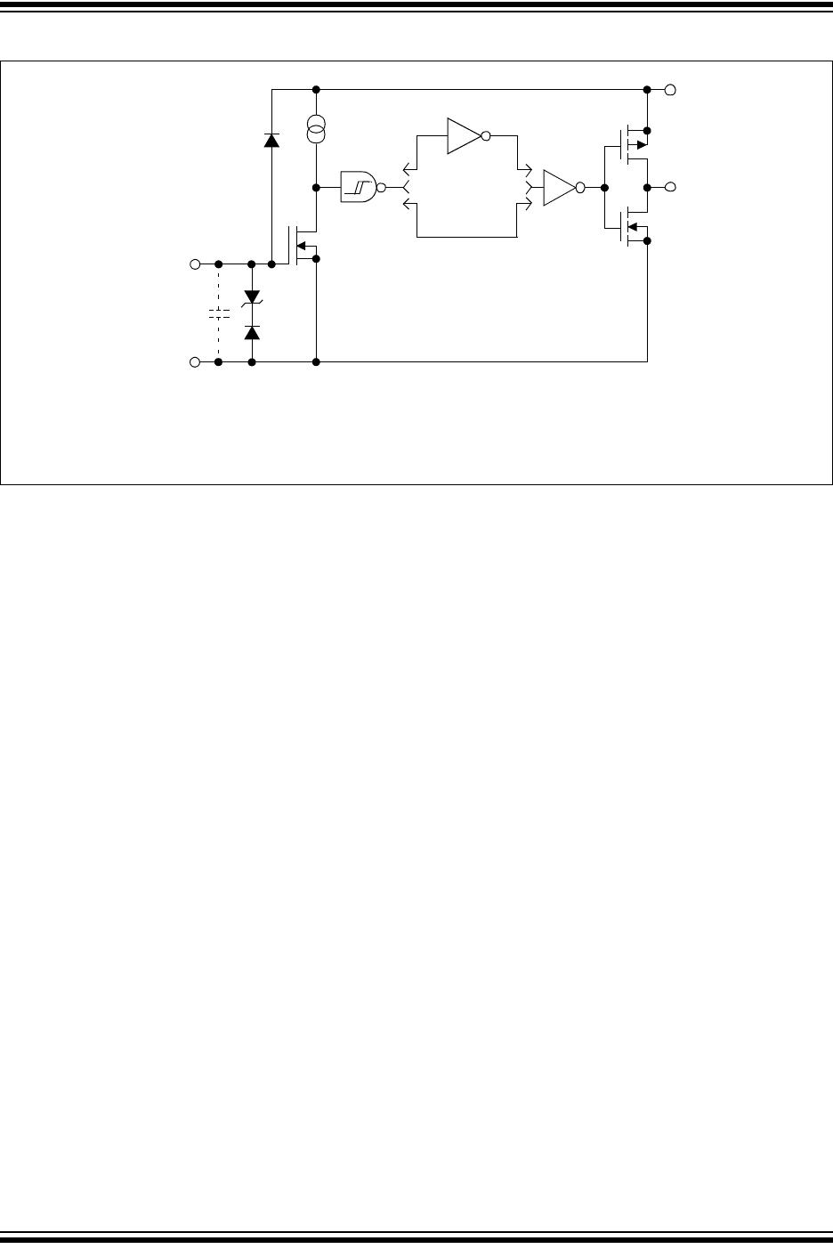
General Description
The TC4426AM/TC4427AM/TC4428AM are improved
versions of the earlier TC4426M/TC4427M/TC4428M
family of MOSFET drivers. In addition to matched rise
and fall times, the TC4426AM/TC4427AM/TC4428AM
devices have matched leading and falling edge
propagation delay times.
These devices are highly latch-up resistant under any
conditions within their power and voltage ratings. They
are not subject to damage when up to 5V of noise
spiking (of either polarity) occurs on the ground pin.
They can accept, without damage or logic upset, up to
500 mA of reverse current (of either polarity) being
forced back into their outputs. All terminals are fully
protected against Electrostatic Discharge (ESD) up to
4kV.
The TC4426AM/TC4427AM/TC4428AM MOSFET
drivers can easily charge/discharge 1000 pF gate
capacitances in under 30 ns, while providing low
enough impedances in both the on and off states to
ensure the MOSFET's intended state will not be
affected, even by large transients.
Package Types
8-Pin CERDIP
1
2
3
4
NC
5
6
7
8
OUT A
OUT B
NC
IN A
GND
IN B
V
DD
TC4426AM
TC4427AM
TC4426AM TC4427AM
NC
OUT A
OUT B
V
DD
TC4428AM
NC
OUT A
OUT B
V
DD
TC4428AM
1.5A Dual High-Speed Power MOSFET Drivers