2005-2013 Microchip Technology Inc. DS21939B-page 7
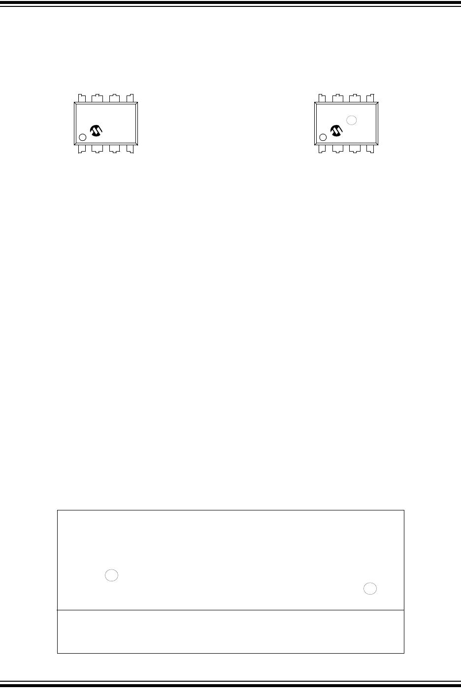
TC4426AM/TC4427AM/TC4428AM
3.0 PIN DESCRIPTIONS
The descriptions of the pins are listed in Table 3-1.
TABLE 3-1: PIN FUNCTION TABLE
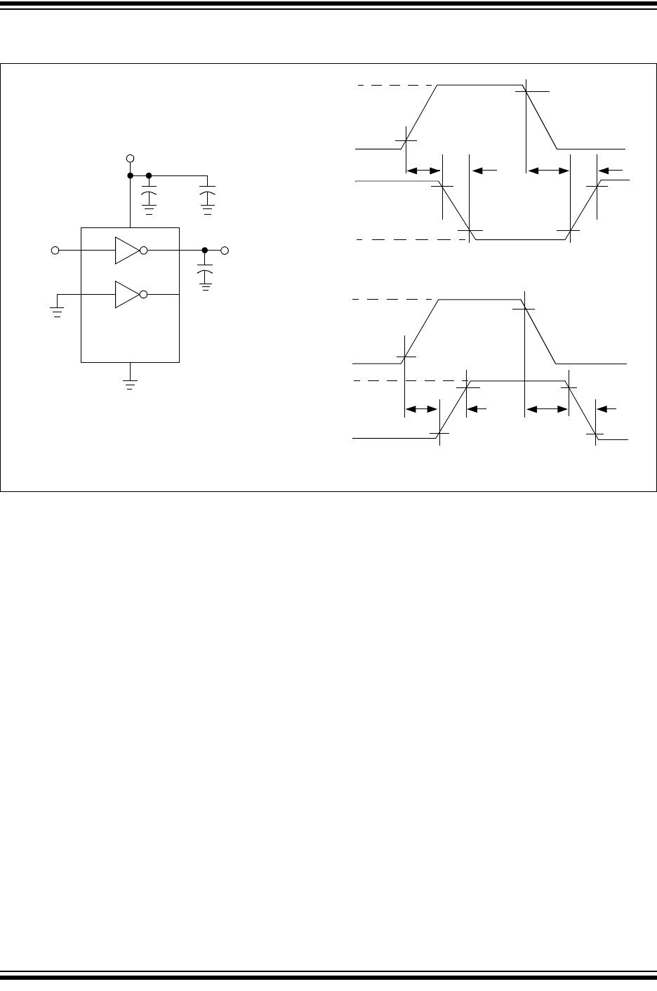
3.1 Inputs A & B (IN A and IN B)
MOSFET driver IN A & B are high-impedance,
TTL/CMOS-compatible inputs. These inputs also have
300 mV of hysteresis between the high and low
thresholds, which prevents output glitching even when
the rise and fall time of the input signal is very slow.
3.2 Ground (GND)
The GND pin is the return path for both the bias current
and the high peak current that discharges the external
load capacitance. The ground pin should be tied into a
ground plane or have a very short trace to the bias sup-
ply source return.
3.3 Outputs A & B (OUT A and OUT B)
MOSFET driver OUT A & B are low-impedance,
CMOS, push-pull style outputs. The pull-down and pull-
up devices are of equal strength, making the rise and
fall times equivalent.
3.4 Supply Input (V
DD
)
The V
DD
input is the bias supply for the MOSFET driver
and is rated for 4.5V to 18V, with respect to the ground
pin. The V
DD
input should be bypassed with local
ceramic capacitors. The value of these capacitors
should be chosen based on the capacitive load that is
being driven.
8-Pin
CERDIP
Symbol Description
1 NC No connection
2 IN A Input A
3 GND Ground
4 IN B Input B
5 OUT B Output B
6V
DD
Supply input
7 OUT A Output A
8 NC No connection