NXP Semiconductors
MF1S70YYX_V1
MIFARE Classic EV1 4K - Mainstream contactless smart card IC for fast and easy solution development
MF1S70yyX_V1 All information provided in this document is subject to legal disclaimers. © NXP B.V. 2017. All rights reserved.
Product data sheet Rev. 3.2 — 23 November 2017
COMPANY PUBLIC 279332 25 / 37
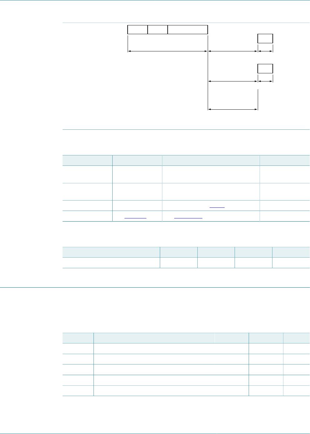
Table 26. MIFARE Increment, Decrement and Restore command
Name Code Description Length
Cmd C1h Increment 1 byte
Cmd C0h Decrement 1 byte
Cmd C2h Restore 1 byte
Addr - MIFARE source block address (00h to FFh) 1 byte
CRC - CRC according to Ref. 4 2 bytes
Data - Operand (4 byte signed integer) 4 bytes
NAK see Table 10 see Section 9.3 4-bit
Table 27. MIFARE Increment, Decrement and Restore timing
T
ACK
min T
ACK
max T
NAK min
T
NAK max
T
TimeOut
Increment,
Decrement, and
Restore part 1
n=9 T
TimeOut
n=9 T
TimeOut
5 ms
Increment,
Decrement, and
Restore part 2
n=9 T
TimeOut
n=9 T
TimeOut
5 ms
Remark: The minimum required time between MIFARE Increment, Decrement, and
Restore part 1 and part 2 is the minimum required FDT according to Ref. 4. There is no
maximum time specified.
Remark: The MIFARE Increment, Decrement, and Restore commands require a
MIFARE Transfer to store the value into a destination block.
Remark: The MIFARE Increment, Decrement, and Restore command part 2 does not
provide an acknowledgement, so the regular time out has to be used instead.
12.5 MIFARE Transfer
The MIFARE Transfer requires a destination block address, and writes the value stored
in the Transfer Buffer into one MIFARE Classic block. The command structure is shown
in Figure 22 and Table 28.
Table 29 shows the required timing.