NB3V110xC Series
www.onsemi.com
7
PARAMETERS MEASUREMENT INFORMATION
Figure 2. Test Load Circuit
Figure 3. Application Load with 50 W Line Termination
Figure 4. Application Load with Series Line Termination
Figure 5. t
DIS
and t
EN
for Disable Low Figure 6. Output Skew t
Sk(o)
Z= 50
O
Ω
R=50 W
from Measurement Equipment
V/2
DD
LVCMOS
Output
V = 3.3 V, 2.5 V or 1.8 V
DD
C=2pF
parasitic capacitance
LVCMOS
Output
V
DD
R=100 W
R=100 W
Z= 50
O
Ω
parasitic input capacitance
V = 3.3 V, 2.5V or 1.8 V
DD
LVCMOS
Output
Z= 50
O
Ω
RS = 10 Ohms (V
DD
= 3.3 V)
RS = 5 Ohms (V
DD
= 2.5 V)
RS = 0 Ohms (V
DD
= 1.8 V)
parasitic input capacitance
V = 3.3 V, 2.5 V or 1.8 V
DD
t
DIS
t
EN
V
IN
/2
OE
Qn
V
IN
/2
t
sk(o)
V
DD
/2
Qn+1
V
DD
/2
Qn
t
sk(o)
NB3V110xC Series
www.onsemi.com
8
t
r
Q
n
80% V
OH
−V
OL
CLKIN
t
f
20% V
OH
−V
OL
V
OH
V
OL
t
PLH
V
DD
/2
Q
n
V
DD
/2
CLKIN
t
PHL
Figure 7. Pulse Skew t
sk(p)
and Propagation Delay
t
PLH
/t
PHL
Figure 8. Rise/Fall Times t
r
/t
f
Note: t
sk(p)
= |t
PLH
− t
PHL
|
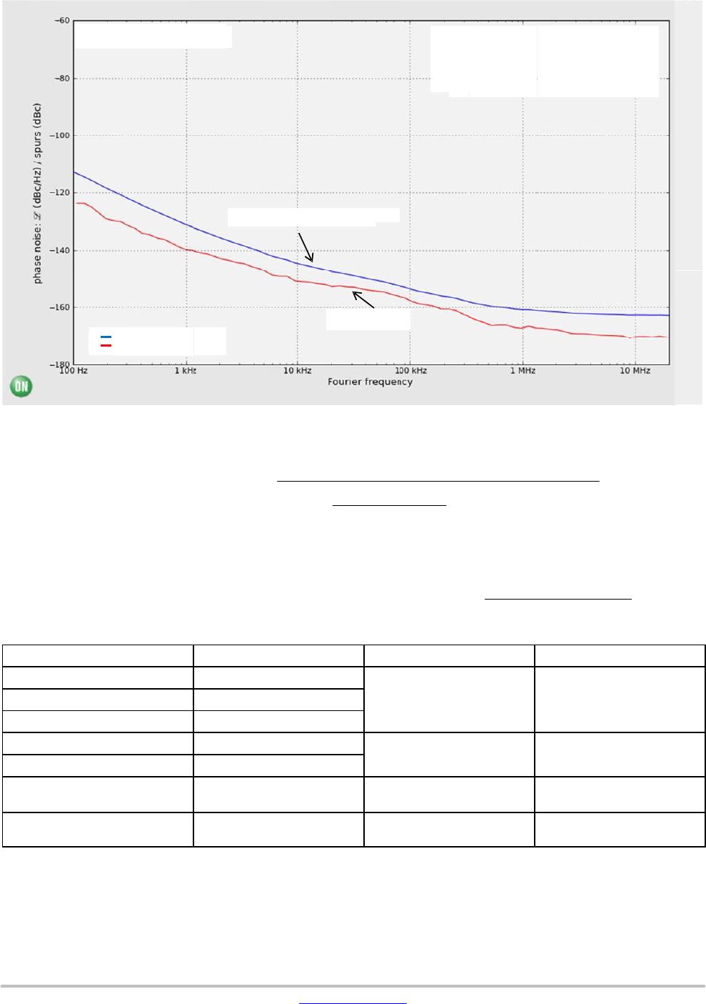
Figure 9. Typical NB3V110xC Phase Noise Plot at f
Carrier
= 100 MHz, V
DD
= 3.3 V, 255C
r
Output
F_carrier = 100 MHz
Output (DUT + Source)
Input Source
Integration Range: 12 kHz − 20 MHz
DUT + Source Phase Jitter = 66.92 fs
Input Source Phase Jitter = 36.72 fs
Input Source 100 MHz
The above phase noise data was captured using Agilent
E5052A/B. The data displays the input phase noise and
output phase noise used to calculate the additive phase jitter
at a specified integration range. The additive RMS phase
jitter contributed by the device (integrated between 12 kHz
and 20 MHz) is 55.94 fs. The additive RMS phase jitter
performance of the fan out buffer is highly dependent on the
phase noise of the input source.
To obtain the most precise additive phase noise
measurement, it is vital that the source phase noise be
notably lower than that of the DUT. If the phase noise of the
source is greater than the noise floor of the device under test,
the source noise will dominate the additive phase jitter
calculation and lead to an incorrect negative result for the
additive phase noise within the integration range. The
Figure above is a good example of the NB3V110xC source
generator phase noise having a significantly lower floor than
the DUT and results in an additive phase jitter of 55.94 fs.
Additive RMS phase jitter + RMS phase jitter of output
2
* RMS phase jitter of input
2
Ǹ
55.94 fs + 66.92 fs
2
* 36.72 fs
2
Ǹ
NB3V110xC Series
www.onsemi.com
9
Figure 10. Typical NB3V110xC Phase Noise Plot at f
Carrier
= 156.25 MHz, V
CC
= 3.3 V V, 255C
u
n
I
r
Input Source
Output (DUT + Source)
Output
Input Source 156.25 MHz
F_carrier = 156.25 MHz
Integration Range: 12 kHz − 20 MHz
DUT + Source Phase Jitter = 51.76 fs
Input Source Phase Jitter = 23.5 fs
The additive RMS phase jitter contributed by the device (integrated between 12 kHz and 20 MHz) is 46.11 fs.
Additive RMS phase jitter + RMS phase jitter of output
2
* RMS phase jitter of input
2
Ǹ
46.11 fs + 51.76 fs
2
* 23.5 fs
2
Ǹ
Figures 9 and 10 were created with measured data from
Agilent−E5052A/B Signal Source Analyzer using ON
Semiconductor Phase Noise Explorer web tool. This free
application enables an interactive environment for advanced
phase noise and jitter analysis of timing devices and clock
tree designs. To see the performance of NB3V110xC
beyond conditions outlined in this datasheet, please visit the
ON Semiconductor Green Point Design Tools
homepage.
Table 8. ORDERING INFORMATION
Device Marking Package Shipping
NB3V1102CDTR2G 102
TSSOP−8
(Pb−Free)
2500 / Tape & Reel
NB3V1103CDTR2G 103
NB3V1104CDTR2G 104
NB3V1102CMTTBG 02
WDFN8
(Pb−Free)
3000 / Tape & Reel
NB3V1104CMTTBG 04
NB3V1106CDTR2G 1106
V
TSSOP−14
(Pb−Free)
2500 / Tape & Reel
NB3V1108CDTR2G 1108
V
TSSOP−16
(Pb−Free)
2500 / Tape & Reel
For information on tape and reel specifications, including part orientation and tape sizes, please refer to our Tape and Reel Packaging
Specifications Brochure, BRD8011/D.
NOTE: Please contact your ON Semiconductor sales representative for availability of parts in tube.

NB3V1102CDTR2G

Mfr. #:
Manufacturer:
ON Semiconductor
Description:
Clock Buffer FANOUT BUFFER WITH 2
Lifecycle:
New from this manufacturer.
Delivery:
DHL FedEx Ups TNT EMS
Payment:
T/T Paypal Visa MoneyGram Western Union