NCP1050, NCP1051, NCP1052, NCP1053, NCP1054, NCP1055
www.onsemi.com
16
APPLICATIONS
Two application examples have been provided in this
document, and they are described in detail in this section.
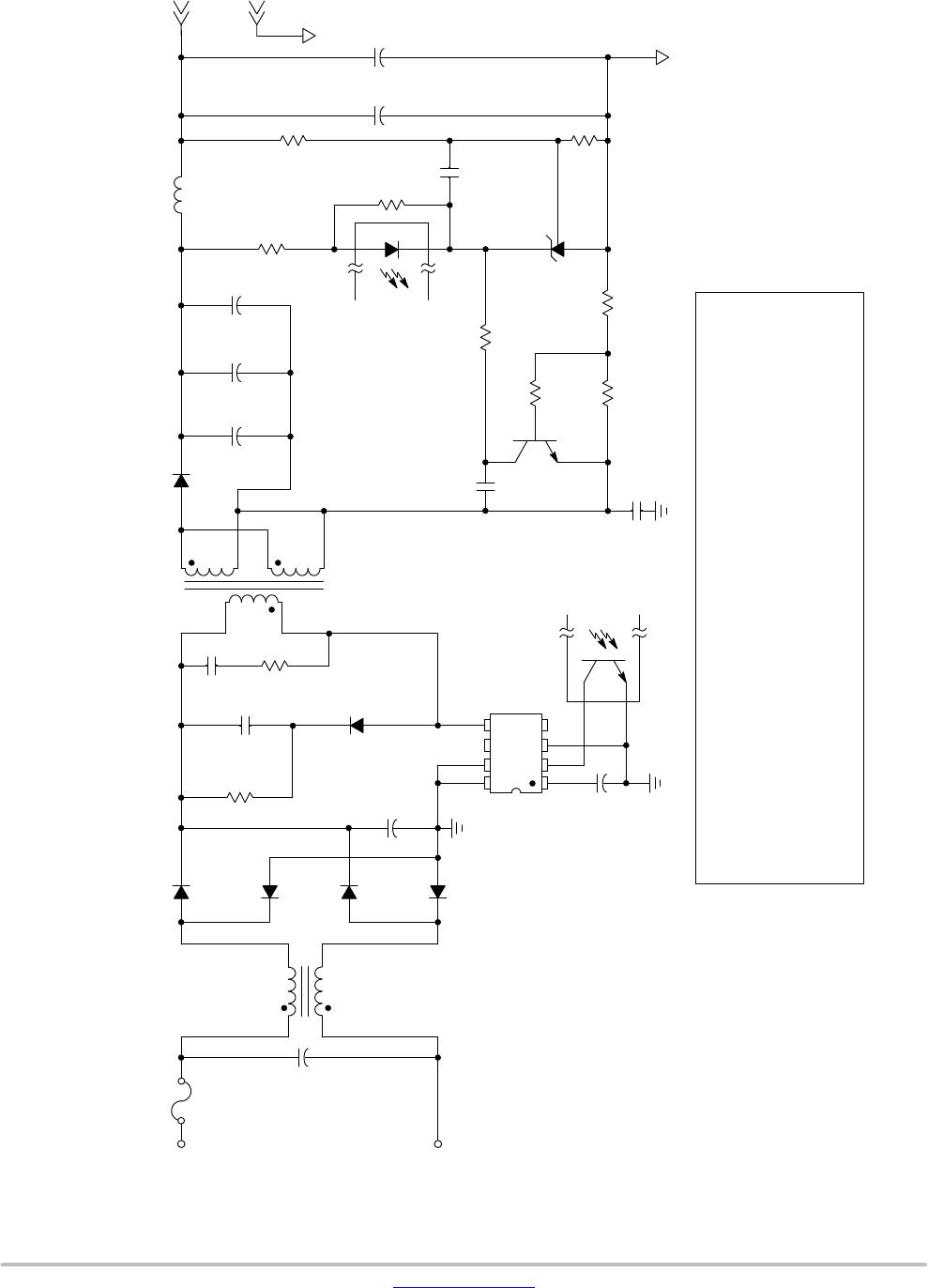
Figure 28 shows a Universal Input, 6 Watt Converter
Application as well as a 5.5 Watt Charger Application using
the NCP1053 @ 100 kHz. The Charger consists of the
additional components Q1, C13, and R7 through R10, as
shown. These were constructed and tested using the printed
circuit board layout shown in Figure 40. The board consists
of a fiberglass epoxy material (FR4) with a single side of two
ounce per square foot (70 m thick) copper foil. Test data
from the two applications is given in Figures 29 through 39.
Both applications generate a well−regulated output
voltage over a wide range of line input voltage and load
current values. The charger application transitions to a
constant current output if the load current is increased
beyond a preset range. This can be very effective for battery
charger application for portable products such as cellular
telephones, personal digital assistants, and pagers. Using the
NCP105X series in applications such as these offers a wide
range of flexibility for the system designer.
The NCP105X application offers a low cost alternative to
other applications. It uses a Dynamic Self−Supply (DSS)
function to generate its own operating supply voltage such
that an auxiliary transformer winding is not needed. (It also
offers the flexibility to override this function with an
auxiliary winding if ultra−low standby power is the
designer’s main concern.) This product also provides for
automatic output overload, short circuit, and open loop
protection by entering a programmable duty cycle burst
mode of operation. This eliminates the need for expensive
devices overrated for power dissipation or maximum
current, or for redundant feedback loops.
The application shown in Figure 28 can be broken down
into sections for the purpose of operating description.
Components C1, L1 and C6 provide EMI filtering for the
design, although this is very dependent upon board layout,
component type, etc. D1 through D4 along with C2 provide
the AC to bulk DC rectification. The NCP1053 drives the
primary side of the transformer, and the capacitor, C5, is an
integral part of the Dynamic Self−Supply. R1, C3, and D5
comprise an RCD snubber and R2 and C4 comprise a ringing
damper both acting together to protect the IC from voltage
transients greater than 700 volts and reduce radiated noise
from the converter. Diode D6 along with C7−9, L2, C11, and
C12 rectify the transformer secondary and filter the output
to provide a tightly regulated DC output. IC3 is a shunt
regulator that samples the output voltage by virtue of R5 and
R6 to provide drive to the optocoupler, IC2, Light Emitting
Diode (LED). C10 is used to compensate the shunt regulator.
When the application is configured as a Charger, Q1 delivers
additional drive to the optocoupler LED when in constant
current operation by sampling the output current through R7
and R8.
Component Selection Guidelines
Choose snubber components R1, C3, and D5 such that the
voltage on pin 5 is limited to the range from 0 to 700 volts.
These components protect the IC from substrate injection if
the voltage was to go below zero volts, and from avalanche
if the voltage was to go above 700 volts, at the cost of slightly
reduced efficiency. For lower power design, a simple RC
snubber as shown, or connected to ground, can be sufficient.
Ensure that these component values are chosen based upon
the worst−case transformer leakage inductance and
worst−case applied voltage. Choose R2 and C4 for best
performance radiated switching noise.
Capacitor C5 serves multiple purposes. It is used along
with the internal startup circuitry to provide power to the IC
in lieu of a separate auxiliary winding. It also serves to
provide timing for the oscillator frequency sweep for
limiting the conducted EMI emissions. The value of C5 will
also determine the response during an output fault (overload
or short circuit) or open loop condition as shown in Figure 4,
along with the total output capacitance.
Resistors R5 and R6 will determine the regulated output
voltage along with the reference voltage chosen with IC3.
The base to emitter voltage drop of Q1 along with the
value of R7 will set the fixed current limit value of the
Charger application. R9 is used to limit the base current of
Q1. Component R8 can be selected to keep the current limit
fixed with very low values of output voltage or to provide
current limit foldback with results as shown in
Figures 29 and 33. A relatively large value of R8 allows for
enough output voltage to effectively drive the optocoupler
LED for fixed current limit. A low value of R8, along with
resistor R10, provides for a low average output power using
the fault protection feature when the output voltage is very
low. C13 provides for output voltage stability when the
Charger application is in current limit.