NCP1050, NCP1051, NCP1052, NCP1053, NCP1054, NCP1055
www.onsemi.com
6
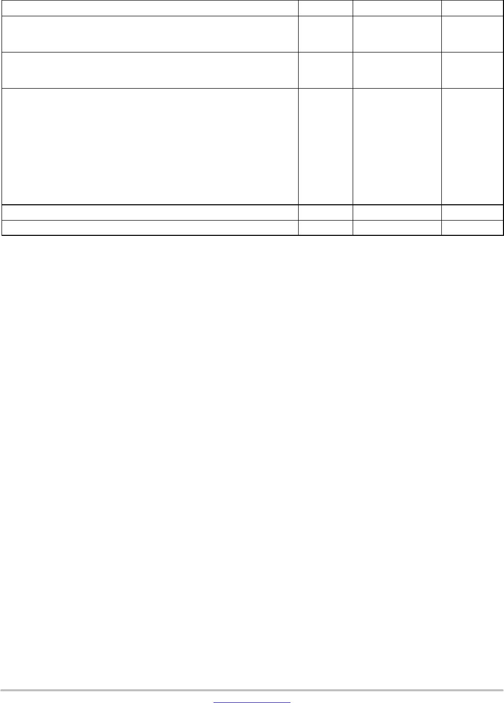
MAXIMUM RATINGS
Rating Symbol Value Unit
Power Switch and Startup Circuit
Drain Voltage Range
Drain Current Peak During Transformer Saturation
V
DS
I
DS(pk)
*0.3 to 700
2.0 x I
lim
Max
V
A
Power Supply/V
CC
Bypass and Control Input
Voltage Range
Current
V
IR
I
max
*0.3 to 10
100
V
mA
Thermal Characteristics
P Suffix, Plastic Package Case 626A−01
Junction−to−Lead
Junction−to−Air, 2.0 Oz. Printed Circuit Copper Clad
0.36 Sq. Inch
1.0 Sq. Inch
ST Suffix, Plastic Package Case 318E−04
Junction−to−Lead
Junction−to−Air, 2.0 Oz. Printed Circuit Copper Clad
0.36 Sq. Inch
1.0 Sq. Inch
R
JL
R
JA
R
JL
R
JA
9.0
77
60
14
74
55
°C/W
Operating Junction Temperature T
J
*40 to +150 °C
Storage Temperature T
stg
*65 to +150 °C
Stresses exceeding those listed in the Maximum Ratings table may damage the device. If any of these limits are exceeded, device functionality
should not be assumed, damage may occur and reliability may be affected.
1. This device series contains ESD protection and exceeds the following tests:
Pins 1−3: Human Body Model 2000 V per JEDEC JESD22−A114−F.
Machine Model Method 400 V per JEDEC JESD22−A115−A.
Pin 5: Human Body Model 1000 V per JEDEC JESD22−A114−F.
Machine Model Method 400 V per JEDEC JESD22−A115−A.
Pin 5 is connected to the power switch and start−up circuits, and is rated only to the max voltage of the part, or 700 V.
Charged Device Model (CDM) 1000 V per JEDEC Standard JESD22−C101E.
2. This device contains Latch−up protection and exceeds $100 mA per JEDEC Standard JESD78.