74LV00 All information provided in this document is subject to legal disclaimers. © NXP Semiconductors N.V. 2015. All rights reserved.
Product data sheet Rev. 4 — 9 December 2015 3 of 14
NXP Semiconductors
74LV00
Quad 2-input NAND gate
5.2 Pin description
6. Functional description
[1] H = HIGH voltage level; L = LOW voltage level; X = don’t care
7. Limiting values
[1] The input and output voltage ratings may be exceeded if the input and output current ratings are observed.
[2] P
tot
derates linearly with 8 mW/K above 70 C.
[3] P
tot
derates linearly with 5.5 mW/K above 60 C.
[4] P
tot
derates linearly with 4.5 mW/K above 60 C.
Table 2. Pin description
Symbol Pin Description
1A to 4A 1, 4, 9, 12 data input
1B to 4B 2, 5, 10, 13 data input
1Y to 4Y 3, 6, 8, 11 data output
GND 7 ground (0 V)
V
CC
14 supply voltage
Table 3. Function table
[1]
Input Output
nA nB nY
LXH
XLH
HHL
Table 4. Limiting values
In accordance with the Absolute Maximum Rating System (IEC 60134). Voltages are referenced to GND (ground = 0 V).
Symbol Parameter Conditions Min Max Unit
V
CC
supply voltage 0.5 +7.0 V
I
IK
input clamping current V
I
< 0.5 V or V
I
>V
CC
+0.5V
[1]
- 20 mA
I
OK
output clamping current V
O
< 0.5 V or V
O
>V
CC
+0.5V
[1]
- 50 mA
I
O
output current V
O
= 0.5 V to (V
CC
+0.5V) - 25 mA
I
CC
supply current - 50 mA
I
GND
ground current 50 - mA
T
stg
storage temperature 65 +150 C
P
tot
total power dissipation T
amb
= 40 C to +125 C
SO14 package
[2]
-500mW
(T)SSOP14 package
[3]
-500mW
DHVQFN14 package
[4]
-500mW
74LV00 All information provided in this document is subject to legal disclaimers. © NXP Semiconductors N.V. 2015. All rights reserved.
Product data sheet Rev. 4 — 9 December 2015 4 of 14
NXP Semiconductors
74LV00
Quad 2-input NAND gate
8. Recommended operating conditions
[1] The static characteristics are guaranteed from V
CC
= 1.2 V to V
CC
= 5.5 V, but LV devices are guaranteed to function down to
V
CC
= 1.0 V (with input levels GND or V
CC
).
9. Static characteristics
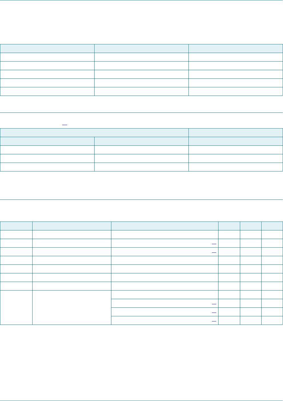
Table 5. Recommended operating conditions
Voltages are referenced to GND (ground = 0 V).
Symbol Parameter Conditions Min Typ Max Unit
V
CC
supply voltage
[1]
1.0 3.3 5.5 V
V
I
input voltage 0 - V
CC
V
V
O
output voltage 0 - V
CC
V
T
amb
ambient temperature 40 +25 +125 C
t/V input transition rise and fall rate V
CC
= 1.0 V to 2.0 V - - 500 ns/V
V
CC
= 2.0 V to 2.7 V - - 200 ns/V
V
CC
= 2.7 V to 3.6 V - - 100 ns/V
V
CC
= 3.6 V to 5.5 V - - 50 ns/V
Table 6. Static characteristics
Voltages are referenced to GND (ground = 0 V).
Symbol Parameter Conditions 40 C to +85 C 40 C to +125 C Unit
Min Typ
[1]
Max Min Max
V
IH
HIGH-level input voltage V
CC
= 1.2 V 0.9 - - 0.9 - V
V
CC
= 2.0 V 1.4 - - 1.4 - V
V
CC
= 2.7 V to 3.6 V 2.0 - - 2.0 - V
V
CC
= 4.5 V to 5.5 V 0.7V
CC
- - 0.7V
CC
-V
V
IL
LOW-level input voltage V
CC
= 1.2 V - - 0.3 - 0.3 V
V
CC
= 2.0 V - - 0.6 - 0.6 V
V
CC
= 2.7 V to 3.6 V - - 0.8 - 0.8 V
V
CC
= 4.5 V to 5.5 V - - 0.3V
CC
-0.3V
CC
V
V
OH
HIGH-level output voltage V
I
= V
IH
or V
IL
I
O
= 100 A; V
CC
= 1.2 V - 1.2 - - - V
I
O
= 100 A; V
CC
= 2.0 V 1.8 2.0 - 1.8 - V
I
O
= 100 A; V
CC
= 2.7 V 2.5 2.7 - 2.5 - V
I
O
= 100 A; V
CC
= 3.0 V 2.8 3.0 - 2.8 - V
I
O
= 100 A; V
CC
= 4.5 V 4.3 4.5 - 4.3 - V
I
O
= 6 mA; V
CC
= 3.0 V 2.4 2.82 - 2.2 - V
I
O
= 12 mA; V
CC
= 4.5 V 3.6 4.2 - 3.5 - V
74LV00 All information provided in this document is subject to legal disclaimers. © NXP Semiconductors N.V. 2015. All rights reserved.
Product data sheet Rev. 4 — 9 December 2015 5 of 14
NXP Semiconductors
74LV00
Quad 2-input NAND gate
[1] Typical values are measured at T
amb
= 25 C.
10. Dynamic characteristics
[1] All typical values are measured at T
amb
=25C.
[2] t
pd
is the same as t
PLH
and t
PHL
.
[3] Typical values are measured at nominal supply voltage (V
CC
= 3.3 V and V
CC
= 5.0 V).
[4] C
PD
is used to determine the dynamic power dissipation (P
D
in W).
P
D
=C
PD
V
CC
2
f
i
N+(C
L
V
CC
2
f
o
) where:
f
i
= input frequency in MHz, f
o
= output frequency in MHz
C
L
= output load capacitance in pF
V
CC
= supply voltage in V
N = number of inputs switching
(C
L
V
CC
2
f
o
) = sum of the outputs.
V
OL
LOW-level output voltage V
I
= V
IH
or V
IL
I
O
= 100 A; V
CC
= 1.2 V - 0 - - - V
I
O
= 100 A; V
CC
= 2.0 V - 0 0.2 - 0.2 V
I
O
= 100 A; V
CC
= 2.7 V - 0 0.2 - 0.2 V
I
O
= 100 A; V
CC
= 3.0 V - 0 0.2 - 0.2 V
I
O
= 100 A; V
CC
= 4.5 V - 0 0.2 - 0.2 V
I
O
= 6 mA; V
CC
= 3.0 V - 0.25 0.40 - 0.50 V
I
O
= 12 mA; V
CC
= 4.5 V - 0.35 0.55 - 0.65 V
I
I
input leakage current V
I
=V
CC
or GND; V
CC
= 5.5 V - - 1.0 - 1.0 A
I
CC
supply current V
I
= V
CC
or GND; I
O
= 0 A;
V
CC
=5.5V
- - 20.0 - 40 A
I
CC
additional supply current per input; V
I
= V
CC
0.6 V;
V
CC
= 2.7 V to 3.6 V
--500-850A
C
I
input capacitance - 3.5 - - - pF
Table 6. Static characteristics …continued
Voltages are referenced to GND (ground = 0 V).
Symbol Parameter Conditions 40 C to +85 C 40 C to +125 C Unit
Min Typ
[1]
Max Min Max
Table 7. Dynamic characteristics
GND = 0 V; For test circuit see Figure 7
.
Symbol Parameter Conditions 40 C to +85 C 40 C to +125 C Unit
Min Typ
[1]
Max Min Max
t
pd
propagation delay nA, nB to nY; see Figure 6
[2]
V
CC
= 1.2 V - 45 - - - ns
V
CC
= 2.0 V - 15 26 - 31 ns
V
CC
= 2.7 V - 11 18 - 23 ns
V
CC
= 3.0 V to 3.6 V; C
L
=15pF
[3]
-7- - -ns
V
CC
= 3.0 V to 3.6 V
[3]
-9.015 - 18ns
V
CC
= 4.5 V to 5.5 V
[3]
-6.511 - 14ns
C
PD
power dissipation
capacitance
C
L
=50pF; f
i
= 1 MHz;
V
I
=GNDtoV
CC
[4]
-22- - -pF

74LV00PW/AUJ

Mfr. #:
Manufacturer:
NXP Semiconductors
Description:
Logic Gates Quad 2-input NAND gate
Lifecycle:
New from this manufacturer.
Delivery:
DHL FedEx Ups TNT EMS
Payment:
T/T Paypal Visa MoneyGram Western Union