NCV7683
www.onsemi.com
15
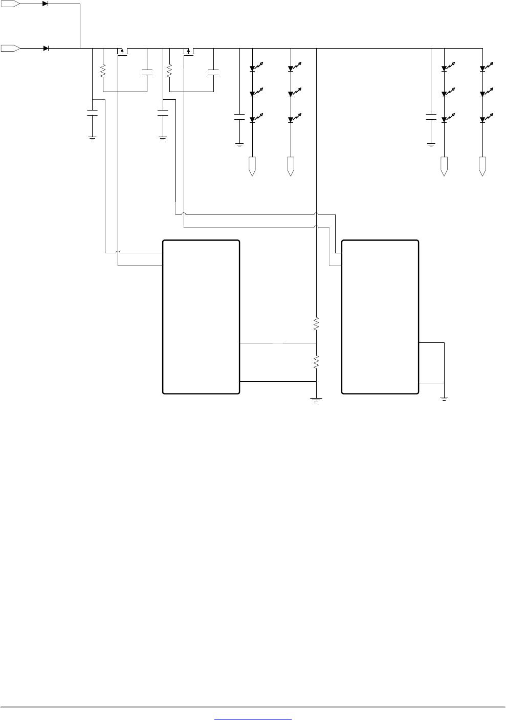
Unused Outputs
Unused outputs should be shorted to ground. The
NCV7683 detects the condition during power−up using the
open load disable threshold and disables the open circuit
detection circuitry. The timing diagrams below highlight the
impacts in time with the sequencing function when an output
is not used. In this example (Figures 26 and 27), OUT7 is not
used and is grounded with SEQ1=0 and SEQ2=0. The
subsequent output (OUT8) has been pulled in (in time) as
shown by the 1st arrow. The 2nd arrow shows the SEQOUT
signal has also been pulled in (in time). For instances which
are coupled with others (in time) (e.g. SEQ1=1 and SEQ2=0
with OUT7 GND), there is no change in the ensuing
waveforms. Figure 27 shows there is no impact for channel
8 when OUT7 is not used.
Figure 26. Unused Output time shift.
(SEQ1=0, SEQ2=0)
Figure 27. Unused Output No Time Shift.
(SEQ1=1, SEQ2=0)
Sequence
Interval
Sequencing_on
SEQOUT
OUT1
(current)
ENABLE
OUT2
(current)
OUT3
(current)
OUT4
(current)
OUT5
(current)
OUT6
(current)
OUT7
(current)
OUT8
(current)
Sequence
Interval
Sequencing_on
SEQOUT
OUT1
(current)
ENABLE
OUT2
(current)
OUT3
(current)
OUT4
(current)
OUT5
(current)
OUT6
(current)
OUT7
(current)
OUT8
(current)
Sequence Time
Sequence Time
*Sequence interval unaffected.
*
*
Sequencing
Output sequencing is controlled by the SEQON,
SEQTIME, SEQ1, and SEQ2 pins. The SEQON pin must be
high to enable any of the sequencing functions. With the
SEQON pin in a low state, all 8 outputs turn on at the same
time and SEQOUT remains high all the time (via the
external pull−up resistor). The SEQ1 and SEQ2
programming pins are utilized by grounding them or leaving
them floating. They follow Table 6 (reference timing
diagrams in Figure 7, Figure 8, Figure 9, and Figure 10). The
sequence interval is defined by the delay of the ENABLE
pin
going low to OUT2 turning on (OUT1 turns on coincident
with ENABLE
). The same sequence time interval is present
for each additional sequential turn−on output of the IC.
Forcing an ENABLE
high or SEQON low will cause a
device which is operating in the sequence mode to leave the
sequence mode. ENABLE
going from low to high
(Figure 28) will turn off all outputs. With SEQON going
high to low (Figure 29 and Figure 30), operation will
continue as a device which is not using the sequence mode
feature. A device which was previously in TAIL mode
(STOP=0) (Figure 29) will revert to TAIL mode. A device
which was previously in STOP mode (STOP=1) Figure 30
will revert to STOP mode.
Before a sequence event, SEQOUT is high impedance.
After a sequence event, SEQOUT is high impedance.
Sequence and Re−Enable Time Programming
Sequence time is programmed using a resistor from the
SEQTIME pin to ground. Figure 21 displays the expected
time using the program resistor. Acceptable values for the
resistor are between 1 K and 10 K. These provide 49 msec
and 490 msec times respectively.
The Sequence Re−Enable Time uses the same internal
timer as the Sequence Time. The Sequence Re−Enable Time
is provided to prevent an immediate feedback triggering in
a daisy chain setup. Reference Figures 33 and Figure 36 for
details.
The program resistor used can be calculated by using the
electrical parameters
1. Sequence Time / R
SEQTIME
2. Sequence Re−Enable Time / R
SEQTIME