NCV7683
www.onsemi.com
4
Table 1. APPLICATION I/O TRUTH TABLE
EN SEQON
STOP
INPUT
TAIL
MODE
OUTx LATCH OFF
(w/ LO
= GND)
OUTX
CURRENT
FAULT
STATE*
DIAG
STATE**
1 X X X no OFF 1
0 0 0 0 no OFF 1
0 0 1 X no I
STOP
NORMAL 0
0 0 1 X no I
STOP
OPEN CIRCUIT*** 1
0 0 1 X yes OFF OPEN CIRCUIT*** 1
0 0 0 1 no PWM NORMAL 0
0 0 0 1 no PWM OPEN CIRCUIT*** PWM
0 1 X X no I
STOP
NORMAL 0
0 1 X X no I
STOP
OPEN CIRCUIT*** 1
0 1 X X yes OFF OPEN CIRCUIT*** 1
Reference Figures below.
X = don’t care
0 = LOW
1 = HIGH
* Open Circuit, RSTOP Current Limit, Set Back Current Limit down 20%, and thermal shutdown
**Pull−up resistor to DIAG and SEQOUT required.
*** OPEN CIRCUIT = Any string or SEQOUT open.
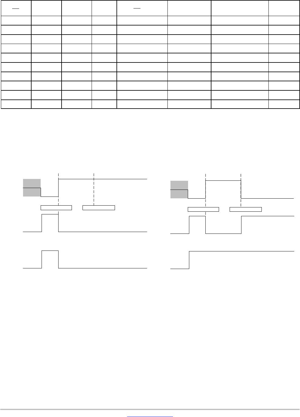
Figure 5. DIAG timing diagram WITH
Open String Latch Active
All outputs latch off.
Figure 6. DIAG timing diagram WITHOUT
Open String Latch Active
No outputs are turned off.
DIAG will report the state.
DIAG
Open String Removed
on
off
on
off
Outputs with no open string.
DIAG
Open String Removed
on
off
on
off
Outputs with no open string.
OUTx
Current
OUTx
Current
Open String Occurs
OUTx
Current
OUTx
Current
Open String Occurs
NCV7683
www.onsemi.com
5
Sequence Programming Timing Diagrams
The four timing diagrams show the options available for sequencing of the 8 outputs dependent on the state of SEQ1 and SEQ2.
1. 8 individual sequence intervals.
2. 4 pairs of sequence intervals.
3. 2 quads of sequence intervals.
4. 1 single sequence interval.
Figure 7. Sequencing Timing Diagram
(SEQ1 = 0, SEQ2 = 0)
Figure 8. Sequencing Timing Diagram
(SEQ1 = 1, SEQ2 = 0)
Figure 9. Sequencing Timing Diagram
(SEQ1 = 0, SEQ2 = 1)
Figure 10. Sequencing Timing Diagram
(SEQ1 = 1, SEQ2 = 1)
Sequence
Interval
Sequencing_on
SEQOUT
OUT1
(current)
ENABLE
OUT2
(current)
OUT3
(current)
OUT4
(current)
OUT5
(current)
OUT6
(current)
OUT7
(current)
OUT8
(current)
Sequence
Interval
Sequencing_on
SEQOUT
OUT1
(current)
ENABLE
OUT2
(current)
OUT3
(current)
OUT4
(current)
OUT5
(current)
OUT6
(current)
OUT7
(current)
OUT8
(current)
Sequence
Interval
Sequencing_on
SEQOUT
OUT1
(current)
ENABLE
OUT2
(current)
OUT3
(current)
OUT4
(current)
OUT5
(current)
OUT6
(current)
OUT7
(current)
OUT8
(current)
Sequencing_on
SEQOUT
OUT1
(current)
ENABLE
OUT2
(current)
OUT3
(current)
OUT4
(current)
OUT5
(current)
OUT6
(current)
OUT7
(current)
OUT8
(current)
Sequence Time
Sequence Time
Sequence Time
Sequence Time
The sequencing function is triggered by a logic level high to low signal on the ENABLE pin.
0=ground
1=floating
NCV7683
www.onsemi.com
6
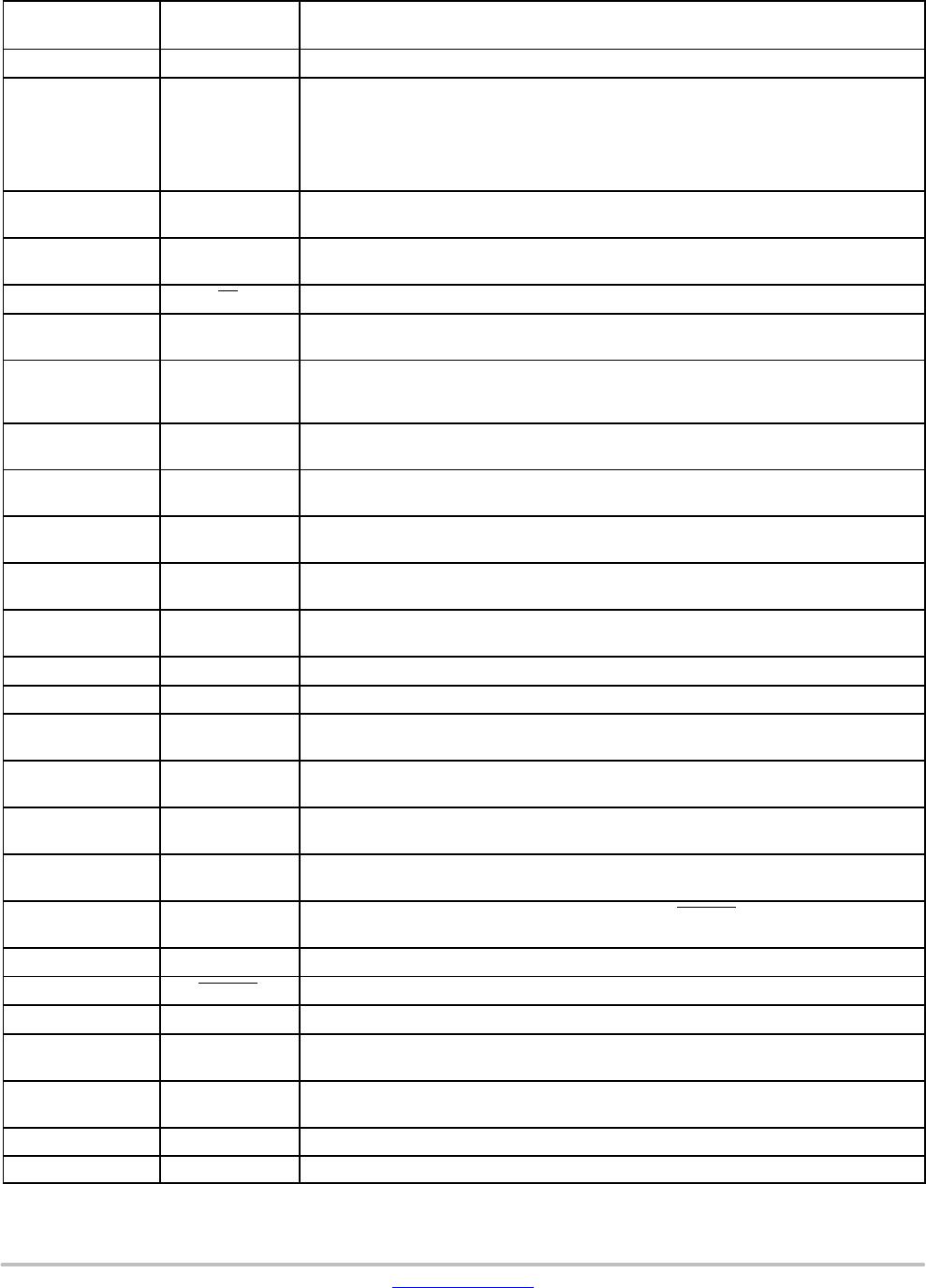
Table 2. PIN FUNCTION DESCRIPTION
SSOP−24 Exposed
Pad Package
Pin # Label Description
1 DIAG Open−drain diagnostic output. Requires a pull−up resistor.
Reporting Open Circuit, RSTOP Current Limit,
Set Back Current Limit down 20%, and thermal shutdown.
Normal Operation = LOW.
Open Load reset input.
Ground if not used (only if latchoff is not used).
2 SEQ1 Grounding this pin changes the output sequencing.
Reference the sequencing section of the datasheet.
3 SEQ2 Grounding this pin changes the output sequencing.
Reference the sequencing section of the datasheet.
4 LO Latch Off. Ground this pin for latch off function.
5 RSTOP Stop current bias program resistor.
Referenced to ground (pin 12).
6 RTAIL Tail current duty cycle PWM program resistor.
Referenced to ground (pin 12).
Ground pin if using external modulation.
7 SEQTIME Sequence Time program resistor.
Referenced to ground (pin 12).
8 OUT8 Channel 8 constant current output to LED.
Unused pin should be grounded (pin 13).
9 OUT7 Channel 7 constant current output to LED.
Unused pin should be grounded (pin 13).
10 OUT6 Channel 6 constant current output to LED.
Unused pin should be grounded (pin 13).
11 OUT5 Channel 5 constant current output to LED.
Unused pin should be grounded (pin 13).
12 GND_Signal Low Current Logic Ground.
13 GND_DRV High Current Driver Ground. Pin is fused to the epad.
14 OUT4 Channel 4 constant current output to LED.
Unused pin should be grounded (pin 13).
15 OUT3 Channel 3 constant current output to LED.
Unused pin should be grounded (pin 13).
16 OUT2 Channel 2 constant current output to LED.
Unused pin should be grounded (pin 13).
17 OUT1 Channel 1 constant current output to LED.
Unused pin should be grounded (pin 13).
18 SEQOUT Open−drain output. Requires a pull−up resistor. Follows ENABLE pin after delay of OUT8
with SEQON high.
19 SEQON High turns on 1−8 output sequencing.
20 ENABLE Global enable input. Low turns device on.
21 VP Supply voltage input.
22 Ballast Drive Gate drive for external power distribution PFET.
Ground if not used.
23 FB Feedback Sense node for VP regulation.
Use feedback resistor divider or connect to GND.
24 STOP Stop Logic Input. External Modulation Input when VP is high.
epad epad Ground. Do not connect to pcb traces other than GND.
NCV7683DQR2G

Mfr. #:
Manufacturer:
ON Semiconductor
Description:
LED Lighting Drivers OCTAL LED DRV SEQUENCING
Lifecycle:
New from this manufacturer.
Delivery:
DHL FedEx Ups TNT EMS
Payment:
T/T Paypal Visa MoneyGram Western Union

Products related to this Datasheet