AD677
REV. A
–9–
in Figure 3. In this circuit BUSY is used to reset the circuitry
which divides the system clock down to provide the AD677
CLK. This serves to interrupt the clock until after the input sig-
nal has been acquired, which has occurred when BUSY goes
HIGH. When the conversion is completed and BUSY goes
LOW, the circuit in Figure 3 truncates the 17th CLK pulse
width which is tolerable because only its rising edge is critical.
5
2
1
7
12
9
4
11
12.288MHz
SYSTEM
CLOCK
CLK
74HC175
2D
1Q
CLR
3D
2Q
3Q
1D
BUSY
CLK
AD677
SAMPLE
2
8
9
12
6
13
1
1QD
74HC393
1CLR
2CLR
2QD
2QC
1CLK
2CLK
Figure 3.
Figure 3 also illustrates the use of a counter (74HC393) to de-
rive the AD677 SAMPLE command from the system clock
when a continuous convert mode is desirable. Pin 9 (2QC) pro-
vides a 96 kHz sample rate for the AD677 when used with a
12.288 MHz system clock. Alternately, Pin 8 (2QD) could be
used for a 48 kHz rate.
If a continuous clock is used, then the user must avoid CLK
edges at the instant of disconnecting V
IN
which occurs at the
falling edge of SAMPLE (see t
FCD
specification). The duty cycle
of CLK may vary, but both the HIGH (t
CH
) and LOW (t
CL
)
phases must conform to those shown in the timing specifica-
tions. The internal comparator makes its decisions on the rising
edge of CLK. To avoid a negative edge transition disturbing the
comparator’s settling, t
CL
should be at least half the value of
t
CLK
. It is not recommended that the SAMPLE pin change state
toward the end of a CLK cycle, in order to avoid transitions dis-
turbing the internal comparator’s settling.
During a conversion, internal dc error terms such as comparator
voltage offset are sampled, stored on internal capacitors and
used to correct for their corresponding errors when needed. Be-
cause these voltages are stored on capacitors, they are subject to
leakage decay and so require refreshing. For this reason there is
a maximum conversion time t
C
(1000 µs). From the time
SAMPLE goes HIGH to the completion of the 17th CLK pulse,
no more than 1000 µs should elapse for specified performance.
However, there is no restriction to the maximum time between
individual conversions.
Output coding for the AD677 is twos complement as shown in
Table I. The AD677 is designed to limit output coding in the
event of out-of-range input.
Table I. Serial Output Coding Format (Twos Complement)
V
IN
Output Code
<Full Scale 011 . . . 11
Full Scale 011 . . . 11
Full Scale – 1 LSB 011 . . . 10
Midscale + 1 LSB 000 . . . 01
Midscale 000 . . . 00
Midscle – 1 LSB 111 . . . 11
–Full Scale + 1 LSB 100 . . . 01
–Full Scale 100 . . . 00
<–Full Scale 100 . . . 00
POWER SUPPLIES AND DECOUPLING
The AD677 has three power supply input pins. V
CC
and V
EE
provide the supply voltages to operate the analog portions of the
AD677 including the capacitor DAC, input buffers and com-
parator. V
DD
provides the supply voltage which operates the
digital portions of the AD677 including the data output buffers
and the autocalibration controller.
As with most high performance linear circuits, changes in the
power supplies can produce undesired changes in the perfor-
mance of the circuit. Optimally, well regulated power supplies
with less than 1% ripple should be selected. The ac output im-
pedance of a power supply is a complex function of frequency,
and in general will increase with frequency. In other words, high
frequency switching such as that encountered with digital cir-
cuitry requires fast transient currents which most power supplies
cannot adequately provide. This results in voltage spikes on the
supplies. If these spikes exceed the ±5% tolerance of the ±12 V
supplies or the ±10% limits of the +5 V supply, ADC perfor-
mance will degrade. Additionally, spikes at frequencies higher
than 100 kHz will also degrade performance. To compensate for
the finite ac output impedance of the supplies, it is necessary to
store “reserves” of charge in bypass capacitors. These capacitors
can effectively lower the ac impedance presented to the AD677
power inputs which in turn will significantly reduce the magni-
tude of the voltage spikes. For bypassing to be effective, certain
guidelines should be followed. Decoupling capacitors, typically
0.1 µF, should be placed as closely as possible to each power
supply pin of the AD677. It is essential that these capacitors be
placed physically close to the IC to minimize the inductance of
the PCB trace between the capacitor and the supply pin. The
logic supply (V
DD
) should be decoupled to digital common and
the analog supplies (V
CC
and V
EE
) to analog common. The ref-
erence input is also considered as a power supply pin in this re-
gard and the same decoupling procedures apply. These points
are displayed in Figure 4.
+5V
+12V –12V
SYSTEM
ANALOG
COMMON
SYSTEM
DIGITAL
COMMON
AGND
DGND
AD677
V
EE
V
CC
V
REF
V
DD
0.1µF
0.1µF
0.1µF
0.1µF
Figure 4. Grounding and Decoupling the AD677
AD677
REV. A
–10–
Additionally, it is beneficial to have large capacitors (>47 µF)
located at the point where the power connects to the PCB with
10 µF capacitors located in the vicinity of the ADC to further
reduce low frequency ripple. In systems that will be subjected to
particularly harsh environmental noise, additional decoupling
may be necessary. RC-filtering on each power supply combined
with dedicated voltage regulation can substantially decrease
power supply ripple effects (this is further detailed in Figure 7).
BOARD LAYOUT
Designing with high resolution data converters requires careful
attention to board layout. Trace impedance is a significant issue.
A 1.22 mA current through a 0.5 trace will develop a voltage
drop of 0.6 mV, which is 4 LSBs at the 16-bit level for a 10 V
full-scale span. In addition to ground drops, inductive and capaci-
tive coupling need to be considered, especially when high accu-
racy analog signals share the same board with digital signals.
Analog and digital signals should not share a common return
path. Each signal should have an appropriate analog or digital
return routed close to it. Using this approach, signal loops en-
close a small area, minimizing the inductive coupling of noise.
Wide PC tracks, large gauge wire, and ground planes are highly
recommended to provide low impedance signal paths. Separate
analog and digital ground planes are also desirable, with a single
interconnection point at the AD677 to minimize interference
between analog and digital circuitry. Analog signals should be
routed as far as possible from digital signals and should cross
them, if at all, only at right angles. A solid analog ground plane
around the AD677 will isolate it from large switching ground
currents. For these reasons, the use of wire wrap circuit con-
struction will not provide adequate performance; careful printed
circuit board construction is preferred.
GROUNDING
The AD677 has three grounding pins, designated ANALOG
GROUND (AGND), DIGITAL GROUND (DGND) and
ANALOG GROUND SENSE (AGND SENSE). The analog
ground pin is the “high quality” ground reference point for the
device, and should be connected to the analog common point in
the system.
AGND SENSE is intended to be connected to the input signal
ground reference point. This allows for slight differences in level
between the analog ground point in the system and the input
signal ground point. However no more than 100 mV is recom-
mended between the AGND and the AGND SENSE pins for
specified performance.
Using AGND SENSE to remotely sense the ground potential of
the signal source can be useful if the signal has to be carried
some distance to the A/D converter. Since all IC ground cur-
rents have to return to the power supply and no ground leads
are free from resistance and inductance, there are always some
voltage differences from one ground point in a system to another.
Over distance this voltage difference can easily amount to sev-
eral LSBs (in a 10 V input span, 16-bit system each LSB is
about 0.15 mV). This would directly corrupt the A/D input sig-
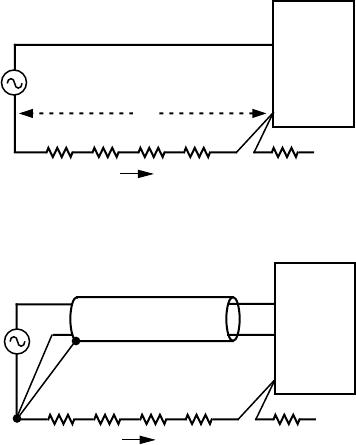
nal if the A/D measures its input with respect to power ground
(AGND) as shown in Figure 5a. To solve this problem the
AD677 offers an AGND SENSE pin. Figure 5b shows how the
AGND SENSE can be used to eliminate the problem in Figure
5a. Figure 5b also shows how the signal wires should be
V
IN
AGND
SOURCE
V
S
GROUND LEAD
I
GROUND
> 0
TO POWER
SUPPLY GND
AD677
V
Figure 5a. Input to the A/D is Corrupted by IR Drop in
Ground Leads: V
IN
= V
S
+
V.
V
IN
AGND
SENSE
AGND
SOURCE
V
S
SHIELDED CABLE
GROUND LEAD
I
GROUND
> 0
TO POWER
SUPPLY GND
AD677
Figure 5b. AGND SENSE Eliminates the Problem in
Figure 5a.
shielded in a noisy environment to avoid capacitive coupling. If
inductive (magnetic) coupling is expected to be dominant such
as where motors are present, twisted-pair wires should be used
instead.
The digital ground pin is the reference point for all of the digital
signals that operate the AD677. This pin should be connected
to the digital common point in the system. As Figure 4 illus-
trated, the analog and digital grounds should be connected
together at one point in the system, preferably at the AD677.
VOLTAGE REFERENCE
The AD677 requires the use of an external voltage reference.
The input voltage range is determined by the value of the refer-
ence voltage; in general, a reference voltage of n volts allows an
input range of ±n volts. The AD677 is specified for a voltage
reference between +5 V and +10 V. A 10 V reference will typi-
cally require support circuitry operated from ±15 V supplies; a
5.0 V reference may be used with ±12 V supplies. Signal-to-
noise performance is increased proportionately with input signal
range (see Figure 12). In the presence of a fixed amount of sys-
tem noise, increasing the LSB size (which results from increas-
ing the reference voltage) will increase the effective S/(N+D)
performance. Figure 11 illustrates S/(N+D) as a function of ref-
erence voltage. In contrast, dc accuracy will be optimal at lower
reference voltage values (such as 5 V) due to capacitor nonlin-
earity at higher voltage values.
During a conversion, the switched capacitor array of the AD677
presents a dynamically changing current load at the voltage ref-
erence as the successive-approximation algorithm cycles through
various choices of capacitor weighting. (See the following sec-
tion “Analog Input” for a detailed discussion of the V
REF
input
characteristics.) The output impedance of the reference circuitry
must be low so that the output voltage will remain sufficiently
constant as the current drive changes. In some applications, this
may require that the output of the voltage reference be buffered
by an amplifier with low impedance at relatively high frequen-
cies. In choosing a voltage reference, consideration should be
AD677
REV. A
–11–
made for selecting one with low noise. A capacitor connected
between REF IN and AGND will reduce the demands on the
reference by decreasing the magnitude of high frequency com-
ponents required to be sourced by the reference.
Figures 6 and 7 represent typical design approaches.
V
IN
10µF
AGND
C
N
1.0µF
+12V
AD586
AD677
6
2
4
8
V
REF
0.1µF
Figure 6.
Figure 6 shows a voltage reference circuit featuring the 5 V out-
put AD586. The AD586 is a low cost reference which utilizes a
buried Zener architecture to provide low noise and drift. Over
the 0°C to +70°C range, the AD586M grade exhibits less than
1.0 mV output change from its initial value at +25°C. A noise
reduction capacitor, C
N
, reduces the broadband noise of the
AD586 output, thereby optimizing the overall performance of
the AD677. It is recommended that a 10 µF to 47 µF high qual-
ity tantalum capacitor and a 0.1 µF capacitor be tied between
the V
REF
input of the AD677 and ground to minimize the im-
pedance on the reference.
Using the AD677 with ±10 V input range (V
REF
= 10 V) typi-
cally requires ±15 V supplies to drive op amps and the voltage
reference. If ±12 V is not available in the system, regulators
such as 78L12 and 79L12 can be used to provide power for the
AD677. This is also the recommended approach (for any input
range) when the ADC system is subjected to harsh environ-
ments such as where the power supplies are noisy and where
voltage spikes are present. Figure 7 shows an example of such a
system based upon the 10 V AD587 reference, which provides a
300 µV LSB. Circuitry for additional protection against power
supply disturbances has been shown. A 100 µF capacitor at each
+15V
+5V
–15V
100µF
100µF
100µF
AD677
10µF
10µF
0.1µF
0.1µF
0.1µF
78L12
79L12
0.01µF
0.01µF
V
IN
V
REF
V
DD
V
CC
V
EE
V
IN
V
O
NR
GND
V
IN
10µF
0.1µF
1µF
AD587
10µF
4
2 6
8
0.1µF
10
10
10
10
Figure 7.
regulator prevents very large voltage spikes from entering the
regulators. Any power line noise which the regulators cannot
eliminate will be further filtered by an RC filter (10 /10 µF)
having a –3 dB point at 1.6 kHz. For best results the regulators
should be within a few centimeters of the AD677.
ANALOG INPUT
As previously discussed, the analog input voltage range for the
AD677 is ±V
REF
. For purposes of ground drop and common
mode rejection, the V
IN
and V
REF
inputs each have their own
ground. V
REF
is referred to the local analog system ground
(AGND), and V
IN
is referred to the analog ground sense pin
(AGND SENSE) which allows a remote ground sense for the
input signal.
The AD677 analog inputs (V
IN
, V
REF
and AGND SENSE) ex-
hibit dynamic characteristics. When a conversion cycle begins,
each analog input is connected to an internal, discharged 50 pF
capacitor which then charges to the voltage present at the corre-
sponding pin. The capacitor is disconnected when SAMPLE is
taken LOW, and the stored charge is used in the subsequent
conversion. In order to limit the demands placed on the external
source by this high initial charging current, an internal buffer
amplifier is employed between the input and this capacitance for
a few hundred nanoseconds. During this time the input pin ex-
hibits typically 20 k input resistance, 10 pF input capacitance
and ±40 µA bias current. Next, the input is switched directly to
the now precharged capacitor and allowed to fully settle. During
this time the input sees only a 50 pF capacitor. Once the sample
is taken, the input is internally floated so that the external input
source sees a very high input resistance and a parasitic input
capacitance of typically only 2 pF. As a result, the only domi-
nant input characteristic which must be considered is the high
current steps which occur when the internal buffers are switched
in and out.
In most cases, these characteristics require the use of an external
op amp to drive the input of the AD677. Care should be taken
with op amp selection; even with modest loading conditions,
most available op amps do not meet the low distortion require-
ments necessary to match the performance capabilities of the
AD677. Figure 8 represents a circuit, based upon the AD845,
which will provide excellent overall performance.
For applications optimized more for low distortion and low
noise, the AD845 of Figure 8 may be replaced by the AD743.
Figure 8.

AD677KRZ

Mfr. #:
Manufacturer:
Analog Devices Inc.
Description:
Analog to Digital Converters - ADC IC 16-BIT Serial 100 kSPS SAMPLING
Lifecycle:
New from this manufacturer.
Delivery:
DHL FedEx Ups TNT EMS
Payment:
T/T Paypal Visa MoneyGram Western Union