AD677
REV. A
–12–
AC PERFORMANCE
AC parameters, which include S/(N+D), THD, etc., reflect the
AD677’s effect on the spectral content of the analog input sig-
nal. Figures 11 through 18 provide information on the AD677’s
ac performance under a variety of conditions.
A perfect n-bit ADC with no errors will yield a theoretical quan-
tization noise of q/√
12, where q is the weight of the LSB. This
relationship leads to the well-known equation for theoretical
full-scale rms sine wave signal-to-noise plus distortion level of
S/(N + D) = 6.02 n + 1.76 dB, here n is the bit resolution. An
actual ADC, however, will yield a measured S/(N + D) less than
the theoretical value. Solving this equation for n using the mea-
sured S/(N + D) value yields the equation for effective number
of bits (ENOB):
ENOB =
S / N + D
()
[]
ACTUAL
–1.76dB
6.02
As a general rule, averaging the results from several conversions
reduces the effects of noise, and therefore improves such param-
eters as S/(N+D). AD677 performance may be optimized by
operating the device at its maximum sample rate of 100 kSPS
and digitally filtering the resulting bit stream to the desired sig-
nal bandwidth. This succeeds in distributing noise over a wider
frequency range, thus reducing the noise density in the fre-
quency band of interest. This subject is discussed in the follow-
ing section.
OVERSAMPLING AND NOISE FILTERING
The Nyquist rate for a converter is defined as one-half its sam-
pling rate. This is established by the Nyquist theorem, which
requires that a signal be sampled at a rate corresponding to at
least twice its highest frequency component of interest in order
to preserve the informational content. Oversampling is a conver-
sion technique in which the sampling frequency is more than
twice the frequency bandwidth of interest. In audio applications,
the AD677 can operate at a 2 × F
S
oversampling rate, where
F
S
= 48 kHz.
In quantized systems, the informational content of the analog
input is represented in the frequency spectrum from dc to the
Nyquist rate of the converter. Within this same spectrum are
higher frequency noise and signal components. Antialias, or low
pass, filters are used at the input to the ADC to reduce these
noise and signal components so that their aliased components
do not corrupt the baseband spectrum. However, wideband
noise contributed by the AD677 will not be reduced by the
antialias filter. The AD677 quantization noise is evenly distrib-
uted from dc to the Nyquist rate, and this fact can be used to
minimize its overall affect.
The AD677 quantization noise effects can be reduced by over-
sampling—sampling at a rate higher than that defined by the
Nyquist theorem. This spreads the noise energy over a band-
width wider than the frequency band of interest. By judicious
selection of a digital decimation filter, noise frequencies outside
the bandwidth of interest may be eliminated.
The process of analog to digital conversion inherently produces
noise, known as quantization noise. The magnitude of this noise
is a function of the resolution of the converter, and manifests it-
self as a limit to the theoretical signal-to-noise ratio achievable.
This limit is described by S/(N + D) = (6.02n + 1.76 + 10 log
F
S
/2F
A
) dB, where n is the resolution of the converter in bits,
F
S
is the sampling frequency, and Fa is the signal bandwidth of
interest. For audio bandwidth applications, the AD677 is ca-
pable of operating at a 2 × oversample rate (96 kSPS), which
typically produces an improvement in S/(N+D) of 3 dB com-
pared with operating at the Nyquist conversion rate of 48 kSPS.
Oversampling has another advantage as well; the demands on
the antialias filter are lessened. In summary, system perfor-
mance is optimized by running the AD677 at or near its maxi-
mum sampling rate of 100 kHz and digitally filtering the
resulting spectrum to eliminate undesired frequencies.
DC PERFORMANCE
The self-calibration scheme used in the AD677 compensates for
bit weight errors that may exist in the capacitor array. This mis-
match in capacitor values is adjusted (using the calibration coef-
ficients) during conversion and provides for excellent dc
linearity performance. Figure 19 illustrates the DNL plot of a
typical AD677 at +25°C. A histogram test is a statistical method
for deriving an A/D converter’s differential nonlinearity. A ramp
input is sampled by the ADC and a large number of conversions
are taken and stored. Theoretically the codes would all be the
same size and, therefore, have an equal number of occurrences.
A code with an average number of occurrences would have a
DNL of “0”. A code with more or less than average will have a
DNL of greater than or less than zero LSB. A DNL of –1 LSB
indicates missing code (zero occurrences).
Figure 20 illustrates the code width distribution of the DNL
plots of Figure 19.
DC CODE UNCERTAINTY
Ideally, a fixed dc input should result in the same output code
for repetitive conversions. However, as a consequence of un-
avoidable circuit noise within the wideband circuits in the ADC,
there is range of output codes which may occur for a given input
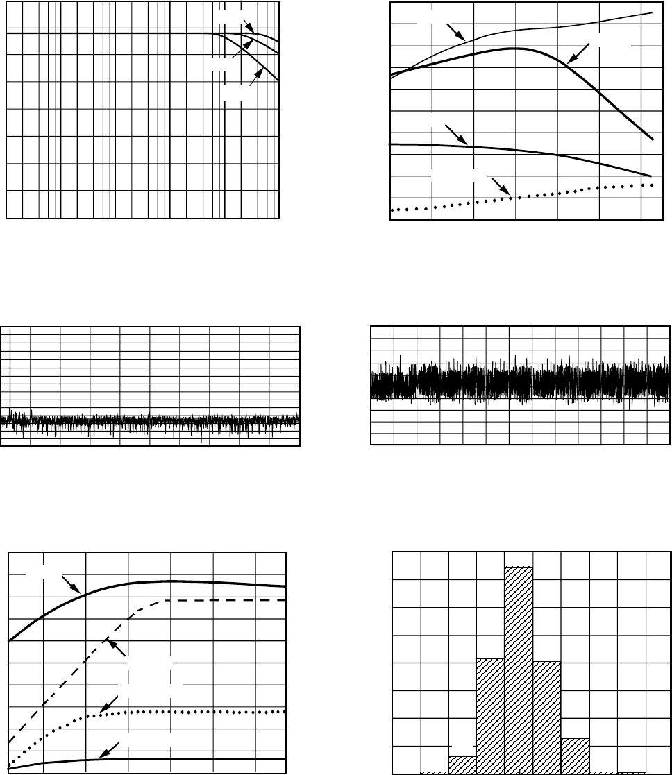
voltage. If you apply a dc signal to the AD677 and record
10,000 conversions, the result will be a distribution of codes as
shown in Figure 9 (using a 10 V reference). If you fit a Gaussian
probability distribution to the histogram, the standard deviation
is approximately equivalent to the rms input noise of ADC.
1
–1
–2
DEVIATION FROM CORRECT CODE – LSBs
NUMBER OF CODE HITS
8000
0
2000
4000
6000
0
7000
5000
3000
1000
3
1267
7649
1081
Figure 9. Distribution of Codes from 10,000 Conversions
Relative to the Correct Code