74HC_HCT03_Q100 All information provided in this document is subject to legal disclaimers. © NXP B.V. 2013. All rights reserved.
Product data sheet Rev. 1 — 4 July 2013 3 of 14
NXP Semiconductors
74HC03-Q100; 74HCT03-Q100
Quad 2-input NAND gate
6. Functional description
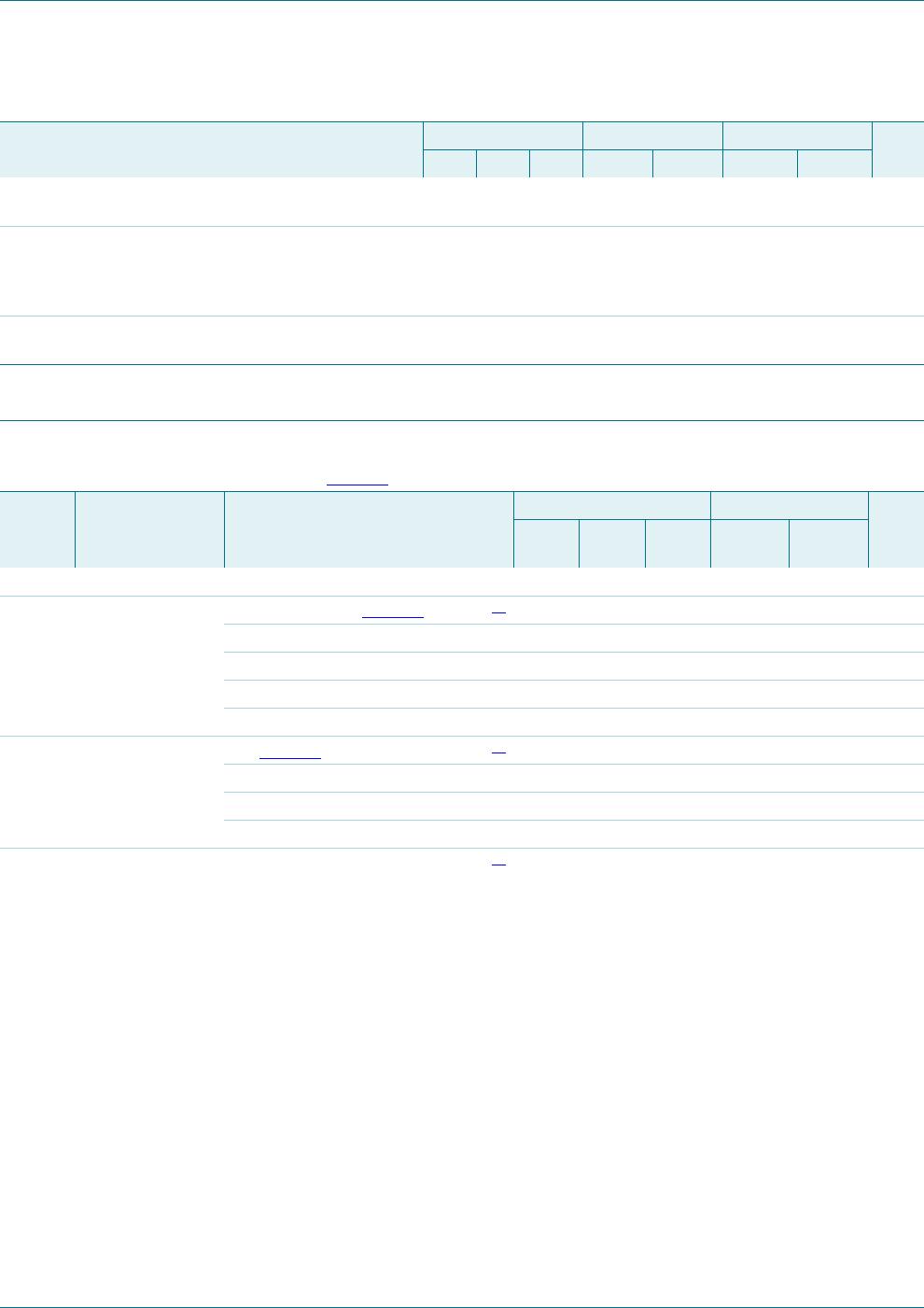
[1] H = HIGH voltage level; L = LOW voltage level; Z = high-impedance OFF-state.
7. Limiting values
[1] The input and output voltage ratings may be exceeded if the input and output current ratings are observed.
[2] For SO14 package: P
tot
derates linearly with 8 mW/K above 70 C.
For (T)SSOP14 packages: P
tot
derates linearly with 5.5 mW/K above 60 C.
8. Recommended operating conditions
Table 3. Function table
[1]
Input Output
nA nB nY
LLZ
LHZ
HLZ
HHL
Table 4. Limiting values
In accordance with the Absolute Maximum Rating System (IEC 60134). Voltages are referenced to GND (ground = 0 V).
Symbol Parameter Conditions Min Max Unit
V
CC
supply voltage 0.5 +7 V
V
O
output voltage
[1]
0.5 +7 V
I
IK
input clamping current V
I
< 0.5 V or V
I
>V
CC
+0.5 V
[1]
- 20 mA
I
OK
output clamping current V
O
< 0.5 V
[1]
- 20 mA
I
O
output current 0.5 V < V
O
- 25 mA
I
CC
supply current - 50 mA
I
GND
ground current 50 - mA
T
stg
storage temperature 65 +150 C
P
tot
total power dissipation
[2]
SO14 and (T)SSOP14
packages
- 500 mW
Table 5. Recommended operating conditions
Voltages are referenced to GND (ground = 0 V)
Symbol Parameter Conditions 74HC03-Q100 74HCT03-Q100 Unit
Min Typ Max Min Typ Max
V
CC
supply voltage 2.0 5.0 6.0 4.5 5.0 5.5 V
V
I
input voltage 0 - V
CC
0-V
CC
V
V
O
output voltage 0 - V
CC
0-V
CC
V
T
amb
ambient temperature 40 +25 +125 40 +25 +125 C
t/V input transition rise and fall rate V
CC
= 2.0 V - - 625 - - - ns/V
V
CC
= 4.5 V - 1.67 139 - 1.67 139 ns/V
V
CC
= 6.0 V - - 83 - - - ns/V
74HC_HCT03_Q100 All information provided in this document is subject to legal disclaimers. © NXP B.V. 2013. All rights reserved.
Product data sheet Rev. 1 — 4 July 2013 4 of 14
NXP Semiconductors
74HC03-Q100; 74HCT03-Q100
Quad 2-input NAND gate
9. Static characteristics
Table 6. Static characteristics
At recommended operating conditions; voltages are referenced to GND (ground = 0 V).
Symbol Parameter Conditions 25 C 40 C to +85 C 40 C to +125 C Unit
Min Typ Max Min Max Min Max
74HC03-Q100
V
IH
HIGH-level
input voltage
V
CC
= 2.0 V 1.5 1.2 - 1.5 - 1.5 - V
V
CC
= 4.5 V 3.15 2.4 - 3.15 - 3.15 - V
V
CC
= 6.0 V 4.2 3.2 - 4.2 - 4.2 - V
V
IL
LOW-level
input voltage
V
CC
= 2.0 V - 0.8 0.5 - 0.5 - 0.5 V
V
CC
= 4.5 V - 2.1 1.35 - 1.35 - 1.35 V
V
CC
= 6.0 V - 2.8 1.8 - 1.8 - 1.8 V
V
OL
LOW-level
output voltage
V
I
= V
IH
or V
IL
I
O
= 20 A; V
CC
= 2.0 V - 0 0.1 - 0.1 - 0.1 V
I
O
= 20 A; V
CC
= 4.5 V - 0 0.1 - 0.1 - 0.1 V
I
O
= 20 A; V
CC
= 6.0 V - 0 0.1 - 0.1 - 0.1 V
I
O
= 4.0 mA; V
CC
= 4.5 V - 0.15 0.26 - 0.33 - 0.4 V
I
O
= 5.2 mA; V
CC
= 6.0 V - 0.16 0.26 - 0.33 - 0.4 V
I
I
input leakage
current
V
I
= V
CC
or GND;
V
CC
=6.0V
-0.1- - 1-1 A
I
OZ
OFF-state
output current
per input pin; V
I
=V
IL
;
V
O
=V
CC
or GND;
other inputs at V
CC
or GND;
V
CC
=6.0V; I
O
=0A
- - ±0.5 - ±5.0 - ±10 A
I
CC
supply current V
I
= V
CC
or GND; I
O
=0A;
V
CC
=6.0V
-2.0- - 20 - 40A
C
I
input
capacitance
-3.5- - - - -pF
74HCT03-Q100
V
IH
HIGH-level
input voltage
V
CC
= 4.5 V to 5.5 V 2.0 1.6 - 2.0 - 2.0 - V
V
IL
LOW-level
input voltage
V
CC
= 4.5 V to 5.5 V - 1.2 0.8 - 0.8 - 0.8 V
V
OL
LOW-level
output voltage
V
I
=V
IH
or V
IL
; V
CC
=4.5V
I
O
=20A - 0 0.1 - 0.1 - 0.1 V
I
O
= 4.0 mA - 0.15 0.26 - 0.33 - 0.4 V
I
I
input leakage
current
V
I
=V
CC
or GND;
V
CC
=5.5V
--0.1 - 1-1 A
I
OZ
OFF-state
output current
per input pin; V
I
=V
IL
;
V
O
=V
CC
or GND;
other inputs at V
CC
or GND;
V
CC
= 5.5 V; I
O
=0A
- - ±0.5 - ±5.0 - ±10 A
74HC_HCT03_Q100 All information provided in this document is subject to legal disclaimers. © NXP B.V. 2013. All rights reserved.
Product data sheet Rev. 1 — 4 July 2013 5 of 14
NXP Semiconductors
74HC03-Q100; 74HCT03-Q100
Quad 2-input NAND gate
10. Dynamic characteristics
I
CC
supply current V
I
= V
CC
or GND; I
O
=0A;
V
CC
=5.5V
--2.0- 20 - 40A
I
CC
additional
supply current
per input pin;
V
I
=V
CC
2.1 V; I
O
=0A;
other inputs at V
CC
or GND;
V
CC
= 4.5 V to 5.5 V
- 100 360 - 450 - 490 A
C
I
input
capacitance
-3.5- - - - -pF
Table 6. Static characteristics
…continued
At recommended operating conditions; voltages are referenced to GND (ground = 0 V).
Symbol Parameter Conditions 25 C 40 C to +85 C 40 C to +125 C Unit
Min Typ Max Min Max Min Max
Table 7. Dynamic characteristics
GND = 0 V; C
L
= 50 pF; for load circuit, see Figure 7.
Symbol Parameter Conditions 25 C 40 C to +125 C Unit
Min Typ Max Max
(85 C)
Max
(125 C)
74HC03-Q100
t
pd
propagation delay nA, nB to nY; see Figure 6
[1]
V
CC
= 2.0 V - 28 95 120 145 ns
V
CC
= 4.5 V - 10 19 24 29 ns
V
CC
= 5.0 V; C
L
=15pF - 8 - - - ns
V
CC
= 6.0 V - 8 16 20 25 ns
t
t
transition time see Figure 6
[2]
V
CC
= 2.0 V - 19 75 95 110 ns
V
CC
= 4.5 V - 7 15 19 22 ns
V
CC
= 6.0 V - 6 13 16 19 ns
C
PD
power dissipation
capacitance
per package; V
I
=GNDtoV
CC
[3]
-4- - -pF

74HCT03PW-Q100J

Mfr. #:
Manufacturer:
Nexperia
Description:
Logic Gates Quad 2-input NAND gate
Lifecycle:
New from this manufacturer.
Delivery:
DHL FedEx Ups TNT EMS
Payment:
T/T Paypal Visa MoneyGram Western Union