74HC_HCT03_Q100 All information provided in this document is subject to legal disclaimers. © NXP B.V. 2013. All rights reserved.
Product data sheet Rev. 1 — 4 July 2013 6 of 14
NXP Semiconductors
74HC03-Q100; 74HCT03-Q100
Quad 2-input NAND gate
[1] t
pd
is the same as t
PLZ
and t
PZL
.
[2] t
t
is the same as t
THL
.
[3] C
PD
is used to determine the dynamic power dissipation (P
D
in W):
P
D
=C
PD
V
CC
2
f
i
N+ (C
L
V
CC
2
f
o
) where:
f
i
= input frequency in MHz;
f
o
= output frequency in MHz;
C
L
= output load capacitance in pF;
V
CC
= supply voltage in V;
N = number of inputs switching;
(C
L
V
CC
2
f
o
) = sum of outputs.
11. Waveforms
74HCT03-Q100
t
pd
propagation delay nA, nB to nY; see Figure 6
[1]
V
CC
= 4.5 V - 12 24 30 36 ns
V
CC
= 5.0 V; C
L
=15pF - 10 - - - ns
t
t
transition time V
CC
= 4.5 V; see Figure 6
[2]
- 7 15 19 22 ns
C
PD
power dissipation
capacitance
per package;
V
I
=GNDtoV
CC
1.5 V
[3]
-4- - -pF
Table 7. Dynamic characteristics …continued
GND = 0 V; C
L
= 50 pF; for load circuit, see Figure 7.
Symbol Parameter Conditions 25 C 40 C to +125 C Unit
Min Typ Max Max
(85 C)
Max
(125 C)
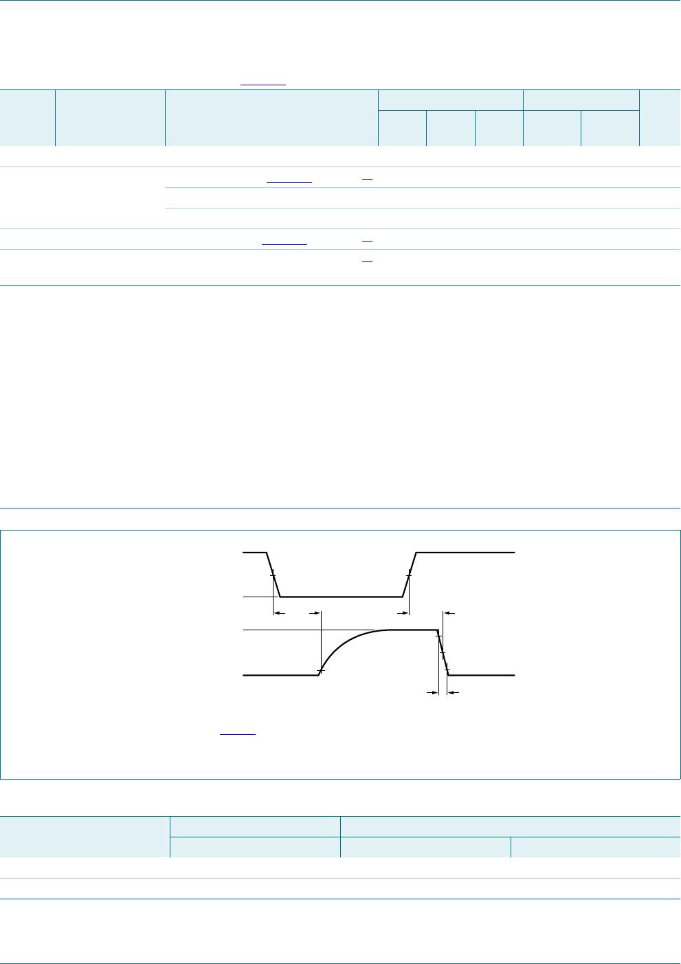
Measurement points are given in Table 8.
V
OL
and V
OH
are typical voltage output levels that occur with the output load.
Fig 6. Input to output propagation delays
DDD
Q$
Q%LQSXW
Q<RXWSXW
9
,
9
&&
9
2/


*1'
9
0
9
0
9
;
W
3/=
W
3=/
W
7+/
Table 8. Measurement points
Type Input Output
V
M
V
M
V
X
74HC03-Q100 0.5V
CC
0.5V
CC
0.1V
CC
74HCT03-Q100 1.3 V 1.3 V 0.1V
CC
74HC_HCT03_Q100 All information provided in this document is subject to legal disclaimers. © NXP B.V. 2013. All rights reserved.
Product data sheet Rev. 1 — 4 July 2013 7 of 14
NXP Semiconductors
74HC03-Q100; 74HCT03-Q100
Quad 2-input NAND gate
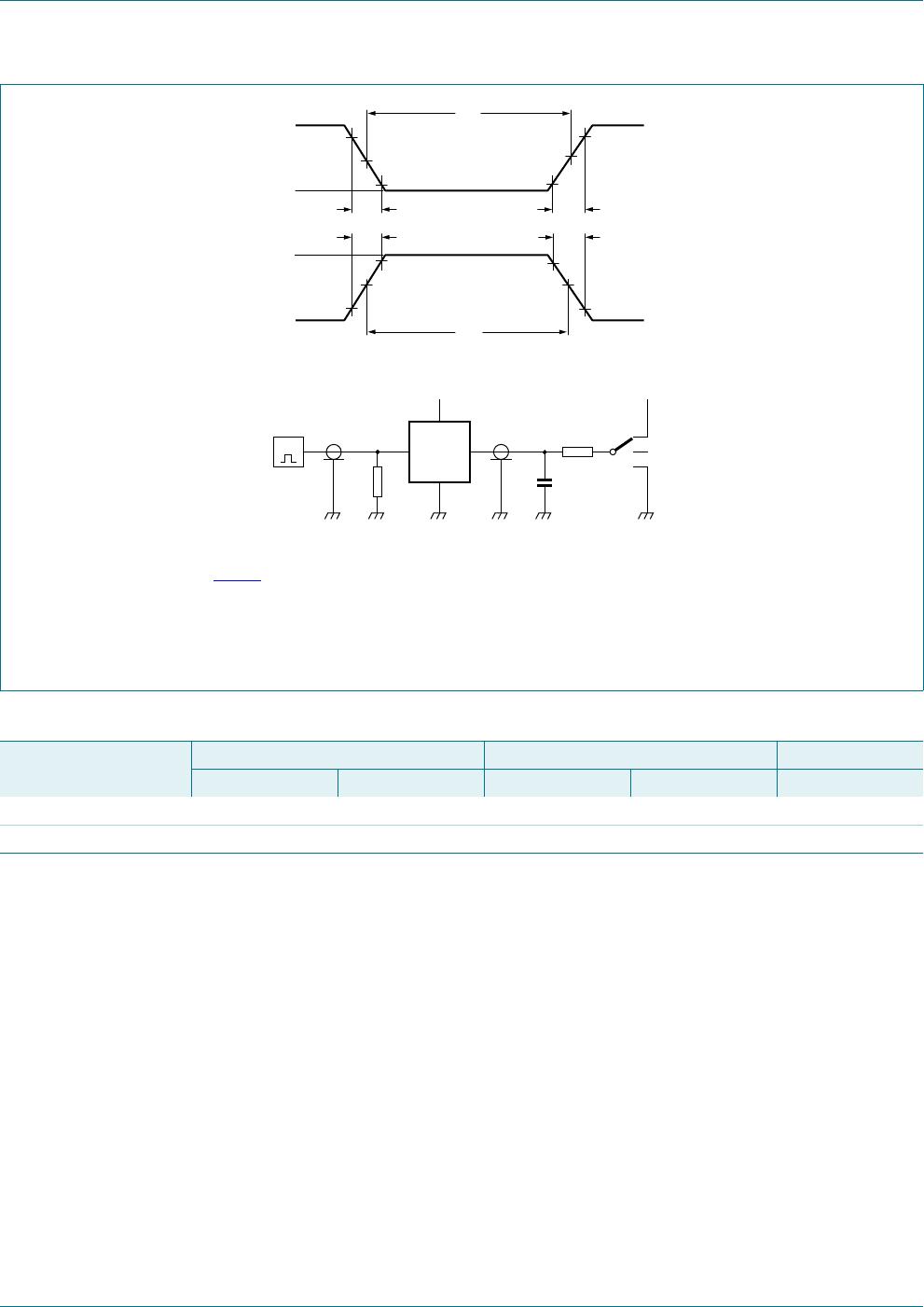
Test data is given in Table 9.
Definitions test circuit:
R
T
= termination resistance should be equal to output impedance Z
o
of the pulse generator.
C
L
= load capacitance including jig and probe capacitance.
Fig 7. Test circuit for measuring switching times
V
M
V
M
t
W
t
W
10 %
90 %
0 V
V
I
V
I
negative
pulse
positive
pulse
0 V
V
M
V
M
90 %
10 %
t
f
t
r
t
r
t
f
001aad983
DUT
V
CC
V
CC
V
I
V
O
R
T
R
L
S1
C
L
open
G
Table 9. Test data
Type Input Load S1 position
V
I
t
r
, t
f
C
L
R
L
t
PZL
, t
PLZ
74HC03-Q100 V
CC
6ns 15pF, 50pF 1k V
CC
74HCT03-Q100 3.0 V 6 ns 15 pF, 50 pF 1 k V
CC
74HC_HCT03_Q100 All information provided in this document is subject to legal disclaimers. © NXP B.V. 2013. All rights reserved.
Product data sheet Rev. 1 — 4 July 2013 8 of 14
NXP Semiconductors
74HC03-Q100; 74HCT03-Q100
Quad 2-input NAND gate
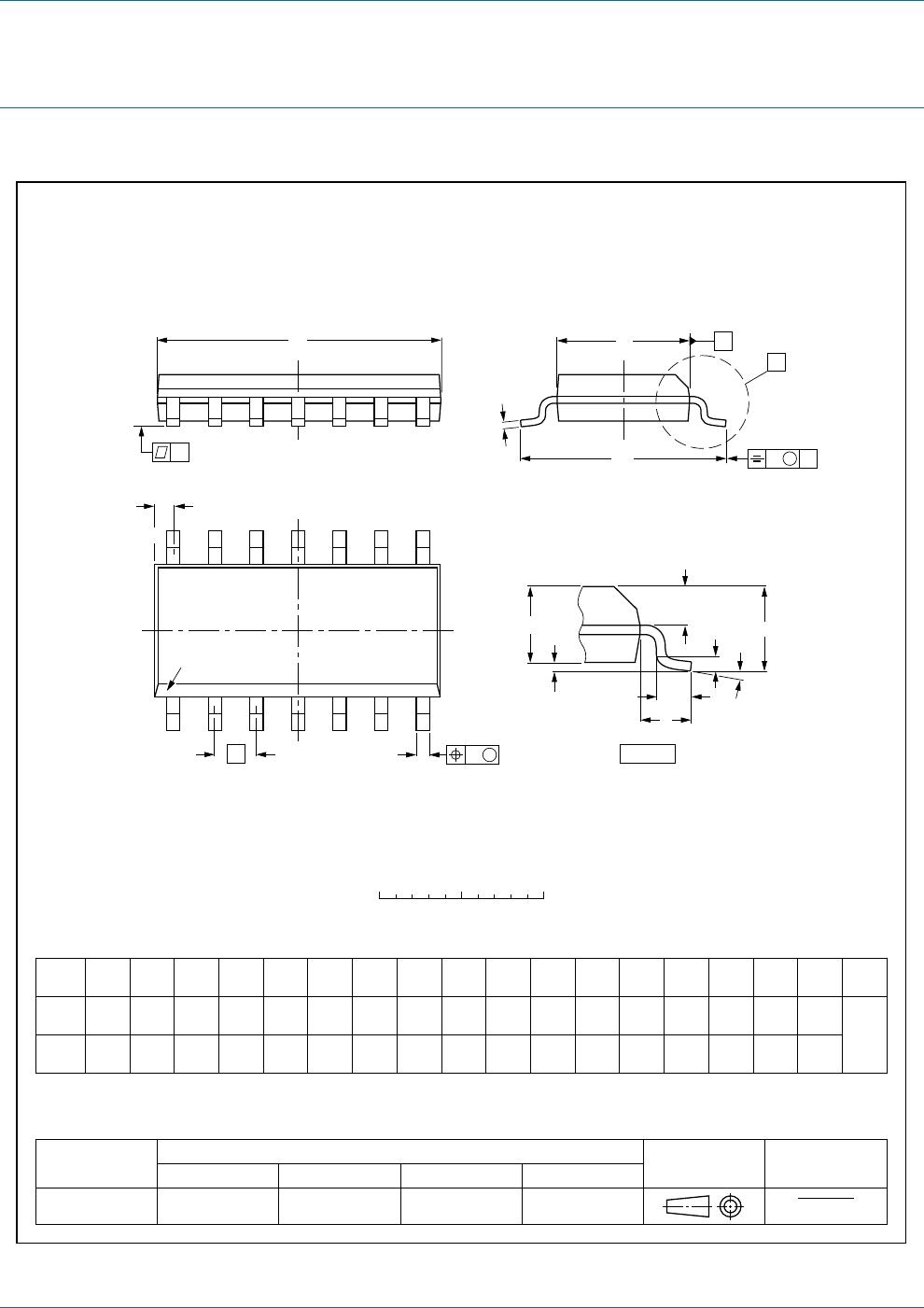
12. Package outline
Fig 8. Package outline SOT108-1 (SO14)
UNIT
A
max.
A
1
A
2
A
3
b
p
cD
(1)
E
(1)
(1)
eH
E
LL
p
QZywv θ
REFERENCES
OUTLINE
VERSION
EUROPEAN
PROJECTION
ISSUE DATE
IEC JEDEC JEITA
mm
inches
1.75
0.25
0.10
1.45
1.25
0.25
0.49
0.36
0.25
0.19
8.75
8.55
4.0
3.8
1.27
6.2
5.8
0.7
0.6
0.7
0.3
8
0
o
o
0.25 0.1
DIMENSIONS (inch dimensions are derived from the original mm dimensions)
Note
1. Plastic or metal protrusions of 0.15 mm (0.006 inch) maximum per side are not included.
1.0
0.4
SOT108-1
X
w M
θ
A
A
1
A
2
b
p
D
H
E
L
p
Q
detail X
E
Z
e
c
L
v M
A
(A )
3
A
7
8
1
14
y
076E06 MS-012
pin 1 index
0.069
0.010
0.004
0.057
0.049
0.01
0.019
0.014
0.0100
0.0075
0.35
0.34
0.16
0.15
0.05
1.05
0.041
0.244
0.228
0.028
0.024
0.028
0.012
0.01
0.25
0.01 0.004
0.039
0.016
99-12-27
03-02-19
0 2.5 5 mm
scale
SO14: plastic small outline package; 14 leads; body width 3.9 mm
SOT108-1

74HCT03PW-Q100J

Mfr. #:
Manufacturer:
Nexperia
Description:
Logic Gates Quad 2-input NAND gate
Lifecycle:
New from this manufacturer.
Delivery:
DHL FedEx Ups TNT EMS
Payment:
T/T Paypal Visa MoneyGram Western Union