SI8806DB-T2-E1

Si8806DB
www.vishay.com
Vishay Siliconix
S16-0637-Rev. E, 18-Apr-16
1
Document Number: 62652
For technical questions, contact: pmostechsupport@vishay.com
THIS DOCUMENT IS SUBJECT TO CHANGE WITHOUT NOTICE. THE PRODUCTS DESCRIBED HEREIN AND THIS DOCUMENT
ARE SUBJECT TO SPECIFIC DISCLAIMERS, SET FORTH AT www.vishay.com/doc?91000
N-Channel 12 V (D-S) MOSFET
Marking Code: xx = AD
xxx = Date/Lot traceability code
Ordering Information:
Si8806DB-T2-E1 (lead (Pb)-free and halogen-free)
FEATURES
TrenchFET
®
power MOSFET
Small 0.8 mm x 0.8 mm outline area
Low 0.4 mm max. profile
Low On-resistance
Material categorization: for definitions of
compliance please see www.vishay.com/doc?99912
APPLICATIONS
Load switch with low voltage drop
• Load switch for low voltage power
lines
Smart phones, tablet PCs, mobile
computing
Notes
a. Surface mounted on 1" x 1" FR4 board with full copper, t = 5 s.
b. Surface mounted on 1" x 1" FR4 board with minimum copper, t = 5 s.
c. Refer to IPC/JEDEC
®
(J-STD-020), no manual or hand soldering.
d. Maximum under steady state conditions is 185 °C/W.
e. Maximum under steady state conditions is 330 °C/W.
PRODUCT SUMMARY
V
DS
(V) R
DS(on)
() MAX. I
D
(A)
a
Q
g
(TYP.)
12
0.047 at V
GS
= 4.5 V 3.9
6.5 nC0.055 at V
GS
= 2.5 V 3.6
0.075 at V
GS
= 1.8 V 3.2
MICRO FOOT
®
0.8 x 0.8
Backside View
1
0.8 mm
0.8 mm
xxx
xx
Bump Side View
1
G
4
D
S
3
S
2
1
G
4
S
3
2
D
S
G
N-Channel MOSFET
ABSOLUTE MAXIMUM RATINGS (T
A
= 25 °C, unless otherwise noted)
PARAMETER SYMBOL LIMIT UNIT
Drain-Source Voltage V
DS
12
V
Gate-Source Voltage V
GS
± 8
Continuous Drain Current (T
J
= 150 °C)
T
A
= 25 °C
I
D
3.9
a
A
T
A
= 70 °C 3.1
a
T
A
= 25 °C 2.8
b
T
A
= 70 °C 2.3
b
Pulsed Drain Current (t = 300 μs) I
DM
20
Continuous Source-Drain Diode Current
T
A
= 25 °C
I
S
0.7
a
T
A
= 25 °C 0.4
b
Maximum Power Dissipation
T
A
= 25 °C
P
D
0.9
a
W
T
A
= 70 °C 0.6
a
T
A
= 25 °C 0.5
b
T
A
= 70 °C 0.3
b
Operating Junction and Storage Temperature Range T
J
, T
stg
-55 to +150
°C
Soldering Recommendations (Peak Temperature)
c
260
THERMAL RESISTANCE RATINGS
PARAMETER SYMBOL TYPICAL MAXIMUM UNIT
Maximum Junction-to-Ambient
a, d
t 5 s R
thJA
105 135
°C/W
Maximum Junction-to-Ambient
b, e
200 260
Si8806DB
www.vishay.com
Vishay Siliconix
S16-0637-Rev. E, 18-Apr-16
2
Document Number: 62652
For technical questions, contact: pmostechsupport@vishay.com
THIS DOCUMENT IS SUBJECT TO CHANGE WITHOUT NOTICE. THE PRODUCTS DESCRIBED HEREIN AND THIS DOCUMENT
ARE SUBJECT TO SPECIFIC DISCLAIMERS, SET FORTH AT www.vishay.com/doc?91000
Notes
a. Pulse test; pulse width 300 μs, duty cycle 2 %.
b. Guaranteed by design, not subject to production testing.
Stresses beyond those listed under “Absolute Maximum Ratings” may cause permanent damage to the device. These are stress ratings only, and functional operation
of the device at these or any other conditions beyond those indicated in the operational sections of the specifications is not implied. Exposure to absolute maximum
rating conditions for extended periods may affect device reliability.
SPECIFICATIONS (T
J
= 25 °C, unless otherwise noted)
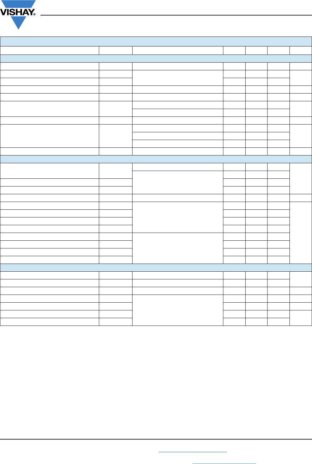
PARAMETER SYMBOL TEST CONDITIONS MIN. TYP. MAX. UNIT
Static
Drain-Source Breakdown Voltage V
DS
V
GS
= 0 V, I
D
= 250 μA 12 - - V
V
DS
Temperature Coefficient V
DS
/T
J
I
D
= 250 μA
-6-
mV/°C
V
GS(th)
Temperature Coefficient V
GS(th)
/T
J
--2.9-
Gate-Source Threshold Voltage V
GS(th)
V
DS
= V
GS
, I
D
= 250 μA 0.4 - 1 V
Gate-Source Leakage I
GSS
V
DS
= 0 V, V
GS
= ± 8 V - - ± 100 nA
Zero Gate Voltage Drain Current I
DSS
V
DS
= 12 V, V
GS
= 0 V - - 1
μA
V
DS
= 12 V, V
GS
= 0 V, T
J
= 55 °C - - 10
On-State Drain Current
a
I
D(on)
V
DS
5 V, V
GS
= 4.5 V 10 - - A
Drain-Source On-State Resistance
a
R
DS(on)
V
GS
= 4.5 V, I
D
= 1 A - 0.035 0.047
V
GS
= 2.5 V, I
D
= 1 A - 0.039 0.055
V
GS
= 1.8 V, I
D
= 0.5 A - 0.047 0.075
Forward Transconductance
a
g
fs
V
DS
= 6 V, I
D
= 1 A - 16 - S
Dynamic
b
Total Gate Charge Q
g
V
DS
= 6 V, V
GS
= 8 V, I
D
= 1 A - 11 17
nC
V
DS
= 6 V, V
GS
= 4.5 V, I
D
= 1 A
-6.510
Gate-Source Charge Q
gs
-0.9-
Gate-Drain Charge Q
gd
-1.6-
Gate Resistance R
g
f = 1 MHz - 6 -
Turn-On Delay Time t
d(on)
V
DD
= 6 V, R
L
= 6
I
D
1 A, V
GEN
= 4.5 V, R
g
= 1
-1020
ns
Rise Time t
r
-2040
Turn-Off Delay Time t
d(off)
-3060
Fall Time t
f
-1225
Turn-On Delay Time t
d(on)
V
DD
= 6 V, R
L
= 6
I
D
1 A, V
GEN
= 8 V, R
g
= 1
-715
Rise Time t
r
-1635
Turn-Off Delay Time t
d(off)
-2550
Fall Time t
f
-920
Drain-Source Body Diode Characteristics
Continuous Source-Drain Diode Current I
S
T
A
= 25 °C - - 0.7
A
Pulse Diode Forward Current I
SM
--20
Body Diode Voltage V
SD
I
S
= 1 A, V
GS
= 0 V - 0.8 1.2 V
Body Diode Reverse Recovery Time t
rr
I
F
= 1 A, dI/dt = 100 A/μs, T
J
= 25 °C
-2040ns
Body Diode Reverse Recovery Charge Q
rr
-510nC
Reverse Recovery Fall Time t
a
-5-
ns
Reverse Recovery Rise Time t
b
-15-
Si8806DB
www.vishay.com
Vishay Siliconix
S16-0637-Rev. E, 18-Apr-16
3
Document Number: 62652
For technical questions, contact: pmostechsupport@vishay.com
THIS DOCUMENT IS SUBJECT TO CHANGE WITHOUT NOTICE. THE PRODUCTS DESCRIBED HEREIN AND THIS DOCUMENT
ARE SUBJECT TO SPECIFIC DISCLAIMERS, SET FORTH AT www.vishay.com/doc?91000
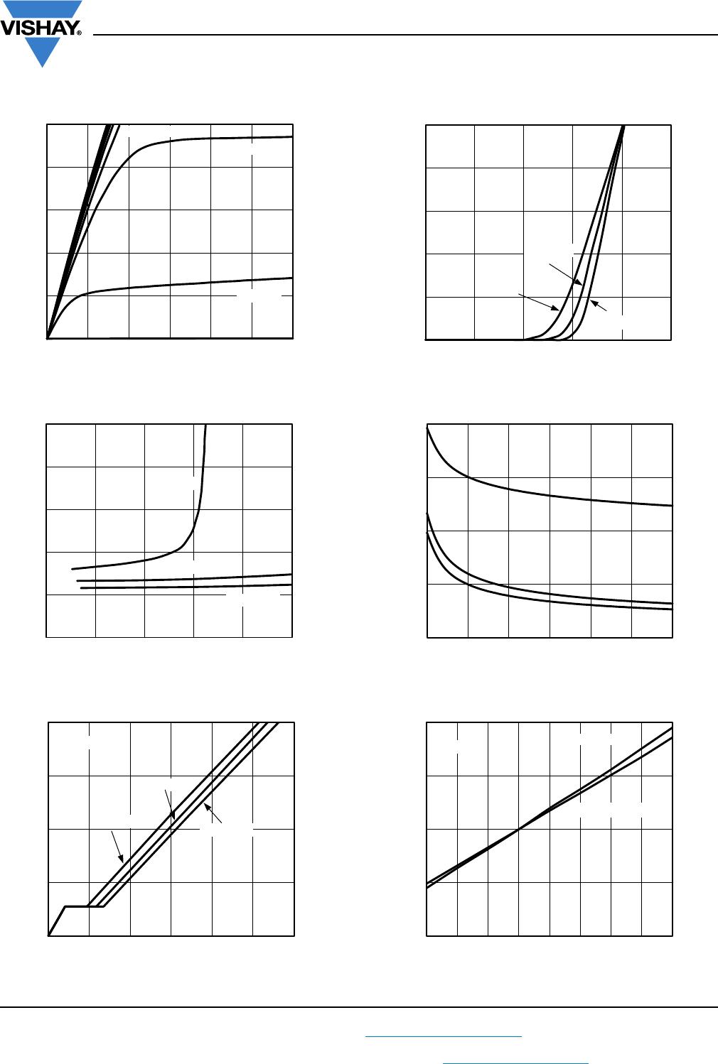
TYPICAL CHARACTERISTICS (25 °C, unless otherwise noted)
Output Characteristics
On-Resistance vs. Drain Current
Gate Charge
Transfer Characteristics
Capacitance
On-Resistance vs. Junction Temperature
0.00
0.03
0.06
0.09
0.12
0.15
0 4 8 12 16 20
R
DS(on)
- On-Resistance (Ω)
I
D
- Drain Current (A)
V
GS
= 4.5 V
V
GS
= 1.8 V
V
GS
= 2.5 V
0
2
4
6
8
0 2 4 6 8 10 12
V
GS
- Gate-to-Source Voltage (V)
Q
g
- Total Gate Charge (nC)
V
DS
= 9.6 V
V
DS
= 3 V
V
DS
= 6 V
I
D
= 1 A
0
2
4
6
8
10
0.0 0.4 0.8 1.2 1.6 2.0
I
D
- Drain Current (A)
V
GS
- Gate-to-Source Voltage (V)
T
C
= 25 °C
T
C
= 125 °C
T
C
= - 55 °C
0
200
400
600
800
0 2 4 6 8 10 12
C - Capacitance (pF)
V
DS
- Drain-to-Source Voltage (V)
C
iss
C
oss
C
rss
0.6
0.8
1.0
1.2
1.4
- 50 - 25 0 25 50 75 100 125 150
R
DS(on)
- On-Resistance (Normalized)
T
J
- Junction Temperature (°C)
V
gs
= 4.5 V
I
d
= 1 A
V
gs
= 2.5 V, 1.8 V

SI8806DB-T2-E1

Mfr. #:
Manufacturer:
Vishay / Siliconix
Description:
MOSFET 12V Vds 8V Vgs MICRO FOOT 0.8 x 0.8
Lifecycle:
New from this manufacturer.
Delivery:
DHL FedEx Ups TNT EMS
Payment:
T/T Paypal Visa MoneyGram Western Union

Products related to this Datasheet