Si8806DB
www.vishay.com
Vishay Siliconix
S16-0637-Rev. E, 18-Apr-16
6
Document Number: 62652
For technical questions, contact: pmostechsupport@vishay.com
THIS DOCUMENT IS SUBJECT TO CHANGE WITHOUT NOTICE. THE PRODUCTS DESCRIBED HEREIN AND THIS DOCUMENT
ARE SUBJECT TO SPECIFIC DISCLAIMERS, SET FORTH AT www.vishay.com/doc?91000
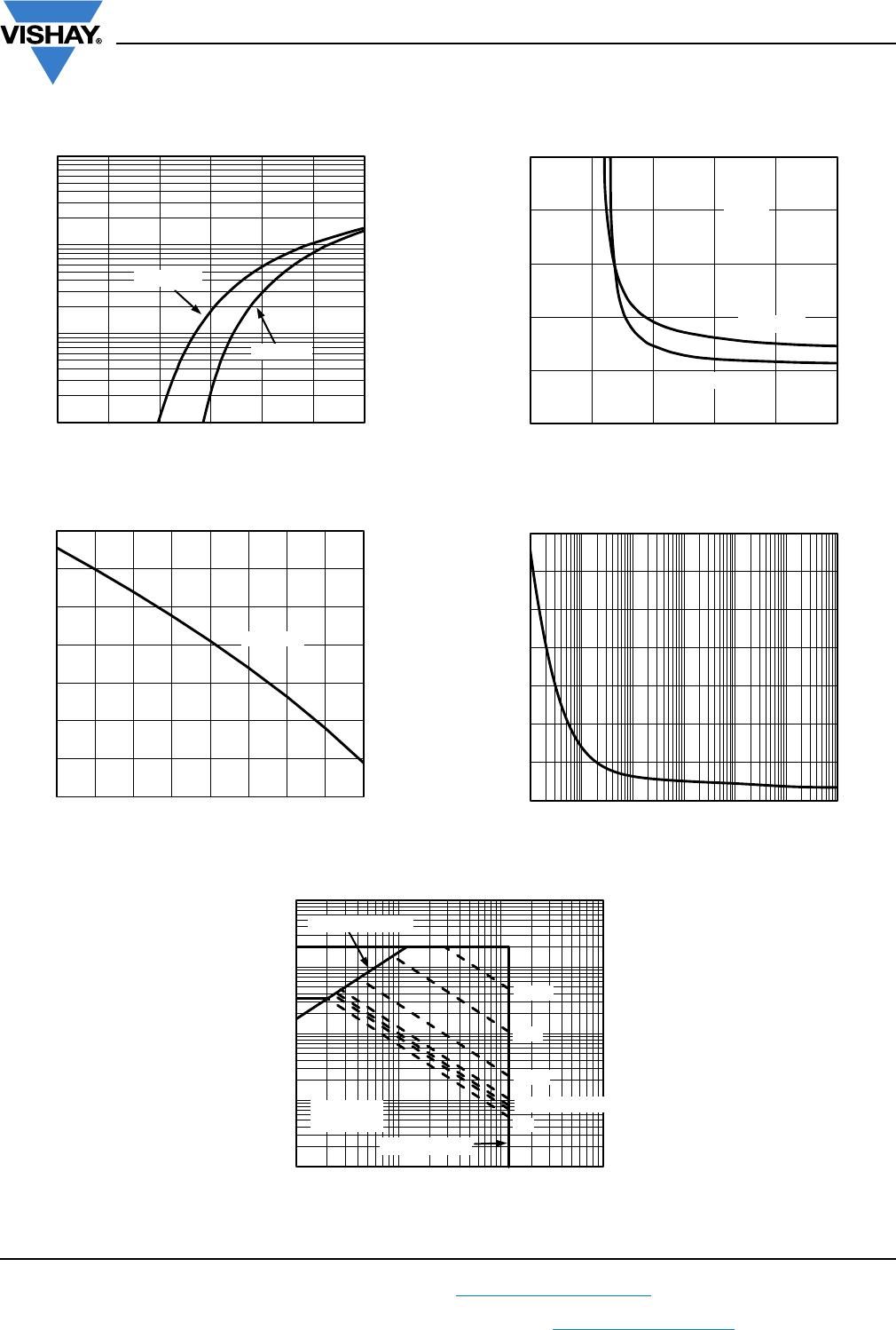
TYPICAL CHARACTERISTICS (25 °C, unless otherwise noted)
Normalized Thermal Transient Impedance, Junction-to-Ambient (On 1" x 1" FR4 Board with Maximum Copper)
Normalized Thermal Transient Impedance, Junction-to-Ambient (On 1" x 1" FR4 Board with Minimum Copper)
Vishay Siliconix maintains worldwide manufacturing capability. Products may be manufactured at one of several qualified locations. Reliability data for Silicon
Technology and Package Reliability represent a composite of all qualified locations. For related documents such as package/tape drawings, part marking, and
reliability data, see www.vishay.com/ppg?62652
.
0.01
0.1
1
0.0001 0.001 0.01 0.1 1 10 100 1000
Normalized Effective Transient
Thermal Impedance
Square Wave Pulse Duration (s)
Duty Cycle = 0.5
0.2
0.1
0.05
0.02
Single Pulse
0.01
0.1
1
0.0001 0.001 0.01 0.1 1 10 100 1000
Normalized Effective Transient
Thermal Impedance
Square Wave Pulse Duration (s)
Duty Cycle = 0.5
0.2
0.1
0.05
0.02
Single Pulse