MAX2140
Complete SDARS Receiver
I
2
C Functional Description
I
2
C Register Map:
This is the standard I
2
C protocol. The first byte is either
C6, C4, C2 (hex) dependent on the state of the I
2
CA_
pins, for a write-to-device operation and either C7, C5,
C3 (hex) for a read-from operation (again dependent
on the state of pins I
2
CA_).
Write Operation:
The first byte is the device address plus the direction
bit (R/W = 0).
The second byte contains the internal address com-
mand of the first address to be accessed.
The third byte is written to the internal register directed
by the command address byte.
The following bytes (if any) are written into successive
internal registers.
The transfer lasts until stop conditions are encountered.
The MAX2140 acknowledges every byte transfer.
Read Operation:
When either address C3, C5, C7 is sent, the MAX2140
sends back first the status byte then the reserved byte.
See Table 5 and Table 6 for read/write register operations.
Layout Issues
The MAX2140 EV kit can be used as a starting point for
layout. For best performance, take into consideration
power-supply issues, as well as the RF, LO, and IF layout.
Power-Supply Layout
To minimize coupling between different sections of the
IC, the ideal power-supply layout is a star configuration,
which has a large decoupling capacitor at a central
V
CC
node. The V
CC
traces branch out from this node,
each going to a separate V
CC
node in the MAX2140
circuit. At the end of each trace is a bypass capacitor
with impedance to ground less than 1Ω at the frequen-
cy of interest. This arrangement provides local decou-
pling at each V
CC
pin. Use at least one via per bypass
capacitor for a low-inductance ground connection.
Matching Network Layout
The layout of a matching network can be very sensitive
to parasitic circuit elements. To minimize parasitic
inductance, keep all traces short and place compo-
nents as close to the IC as possible. To minimize para-
sitic capacitance, a cutout in the ground plane (and
any other planes) below the matching network compo-
nents can be used. On the high-impedance ports (e.g.,
IF inputs and outputs), keep traces short to minimize
shunt capacitance.
Chip Information
TRANSISTOR COUNT: 22,000
PROCESS: BiCMOS
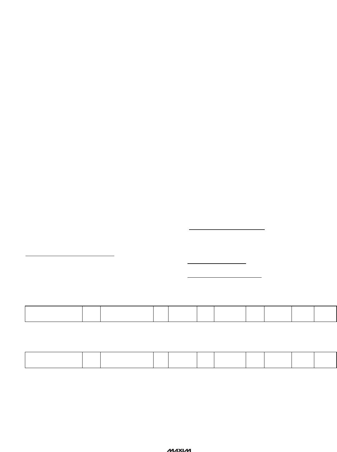
Table 6. Example: Read from Status Registers (Sending an NACK Terminate Slave
Transmit Mode
Maxim cannot assume responsibility for use of any circuitry other than circuitry entirely embodied in a Maxim product. No circuit patent licenses are
implied. Maxim reserves the right to change the circuitry and specifications without notice at any time.
13 ____________________Maxim Integrated Products, 120 San Gabriel Drive, Sunnyvale, CA 94086 408-737-7600
© 2005 Maxim Integrated Products Printed USA is a registered trademark of Maxim Integrated Products, Inc.
Package Information
For the latest package outline information, go to
www.maxim-ic.com/packages
.