TJA1028 All information provided in this document is subject to legal disclaimers. © NXP B.V. 2012. All rights reserved.
Product data sheet Rev. 4 — 25 July 2012 4 of 24
NXP Semiconductors
TJA1028
LIN transceiver with integrated voltage regulator
6. Pinning information
6.1 Pinning
6.2 Pin description
[1] For enhanced thermal and electrical performance, the exposed center pad of the HVSON8 package should
be soldered to board ground (and not to any other voltage level).
7. Functional description
The TJA1028 combines the functionality of a LIN transceiver and a voltage regulator in a
single chip and offers wake-up by bus activity. The voltage regulator is designed to power
the Electronic Control Unit’s (ECU) microcontroller and its peripherals.
The LIN transceiver is the interface between a LIN master/slave protocol controller and
the physical bus in a LIN network. According to the Open System Interconnect (OSI)
model, these modules make up the LIN physical layer.
a. TJA1028T/xxx/xx: SO8 b. TJA1028TK/xxx/xx: HVSON8
Fig 2. Pin configuration diagrams
TJA1028T
V
BAT
V
CC
EN
GND
TXD
LIN RXD
015aaa082
1
2
3
4
6
5
8
7
RSTN
015aaa244
TJA1028TK
RXD
GND
LIN
TXD
EN RSTN
V
BAT
V
CC
Transparent top view
4
5
3 6
2 7
1 8
terminal 1
index area
Table 3. Pin description
Symbol Pin Description
V
BAT
1 battery supply for the TJA1028
EN 2 enable input
GND 3
[1]
ground
LIN 4 LIN bus line
RXD 5 LIN receive data output
TXD 6 LIN transmit data input
RSTN 7 reset output (active LOW)
V
CC
8 voltage regulator output
TJA1028 All information provided in this document is subject to legal disclaimers. © NXP B.V. 2012. All rights reserved.
Product data sheet Rev. 4 — 25 July 2012 5 of 24
NXP Semiconductors
TJA1028
LIN transceiver with integrated voltage regulator
The TJA1028T/xxx/20 and TJA1028TK/xxx/20 versions are optimized for a transmission
speed of 20 kBd, the maximum specified in the LIN standard. The TJA1028T/xxx/10 and
TJA1028TK/xxx/10 versions are optimized for a transmission speed of 10.4 kBd, as
specified in SAE J2602. All versions achieve optimum ElectroMagnetic Compatibility
(EMC) performance by wave shaping the LIN output.
7.1 LIN 2.x/SAE J2602 compliant
The TJA1028 is fully LIN 2.0, LIN 2.1, LIN 2.2 and SAE J2602 compliant. Since the LIN
physical layer is independent of higher OSI model layers (e.g. the LIN protocol), nodes
containing a LIN 2.2-compliant physical layer can be combined, without restriction, with
LIN physical layer nodes that comply with earlier revisions (i.e. LIN 1.0, LIN 1.1, LIN 1.2,
LIN 1.3, LIN 2.0 and LIN 2.1).
7.2 Operating modes
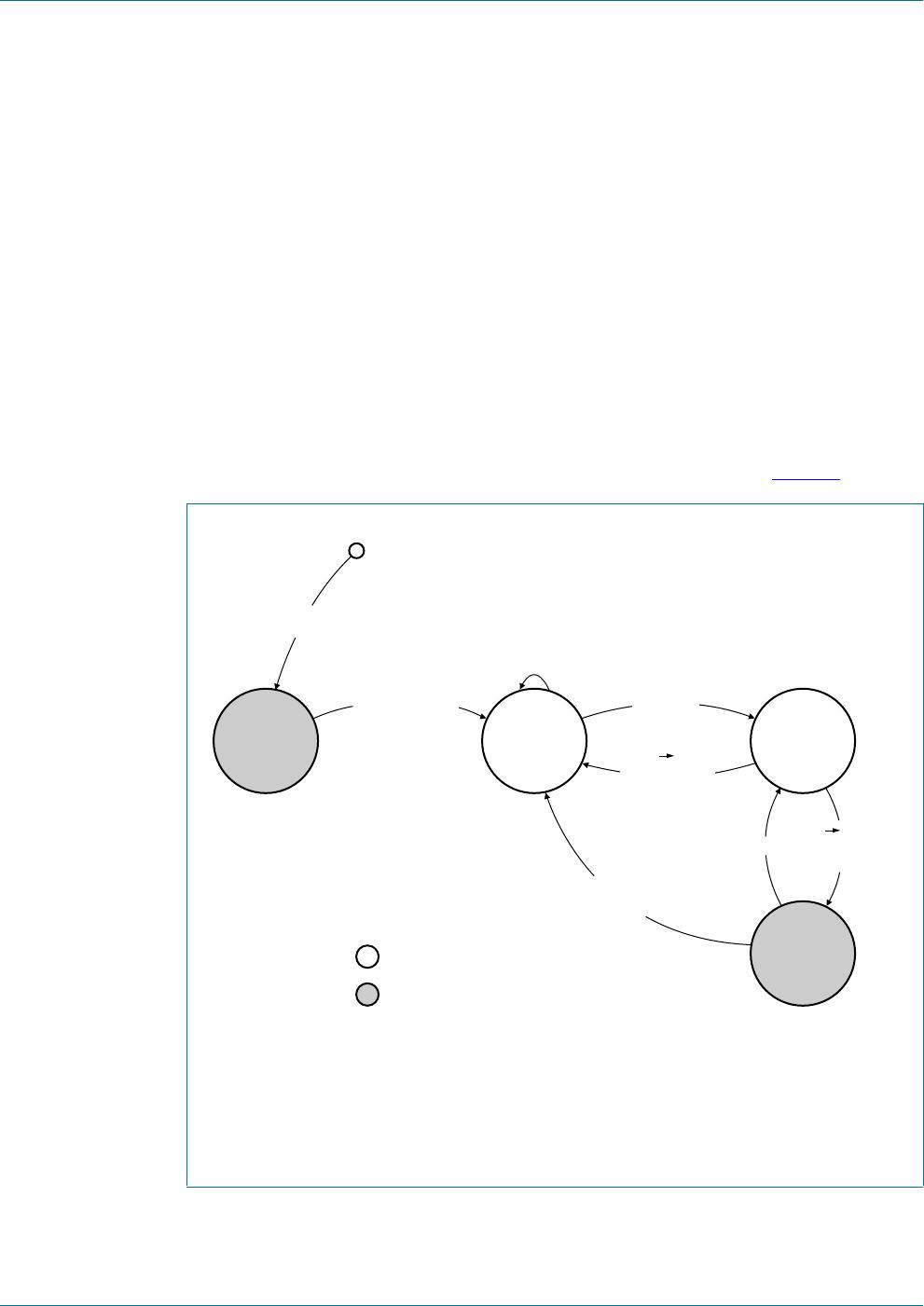
The TJA1028 supports four operating modes: Normal, Standby, Sleep and Off. The
operating modes, and the transitions between modes, are illustrated in Figure 3
.
(1) In Normal mode, the LIN transmitter is enabled - but if EN and/or RSTN go LOW, the LIN
transmitter will be disabled. Remote wake-up signalling will be activated.
(2) Until V
CC
drops below 2 V.
(3) If a wake-up event and a go-to-sleep event occur simultaneously, the device will switch directly to
Standby mode without initiating a reset.
Fig 3. State diagram
NORMAL
(1)
LIN = on
STANDBY
LIN = off
(RXD signals
wake source)
AII states
OFF
LIN = off
RXD = floating
RSTN = LOW
V
BAT
> V
th(det)pon AND
T
vj
< T
th(rel)otp
Voltage regulator
- on
Voltage regulator
- off
wake-up
(3)
event
015aaa086
EN = 1 AND
RSTN = 1
EN = 1 0 AND
(3)
TXD = 0 AND
RSTN = 1
EN = 1
EN = 1 0 AND
TXD = 1 AND
RSTN = 1
V
BAT
< V
th(det)poff
OR
T
vj
> T
th(act)otp
SLEEP
LIN = off
RXD = V
CC
(2)
RSTN = LOW
remote
wake-up
TJA1028 All information provided in this document is subject to legal disclaimers. © NXP B.V. 2012. All rights reserved.
Product data sheet Rev. 4 — 25 July 2012 6 of 24
NXP Semiconductors
TJA1028
LIN transceiver with integrated voltage regulator
7.2.1 Off mode
The TJA1028 switches to Off mode from all other modes if the battery supply voltage
drops below the power-off detection threshold (V
th(det)poff
) or the junction temperature
exceeds the overtemperature protection activation threshold (T
th(act)otp
).
The voltage regulator and the LIN physical layer are disabled in Off mode, and pin RSTN
is forced LOW.
7.2.2 Standby mode
Standby mode is a low-power mode that guarantees very low current consumption.
The TJA1028 switches from Off mode to Standby mode as soon as the battery supply
voltage rises above the power-on detection threshold (V
BAT
> V
th(det)pon
), provided the
junction temperature is below the overtemperature protection release threshold
(T
vj
<T
th(rel)otp
).
The TJA1028 switches to Standby mode from Normal mode during the mode select
window if TXD is HIGH and EN is LOW (see Section 7.2.5
), provided RSTN = 1.
A remote wake-up event will trigger a transition to Standby mode from Sleep mode. The
remote wake-up event will be signalled by a continuous LOW level on pin RXD.
In Standby mode, the voltage regulator is on, the LIN physical layer is disabled and
remote wake-up detection is active. The wake-up source is indicated by the level on RXD
(LOW indicates a remote wake-up).
7.2.3 Normal mode
If the EN pin is pulled HIGH while the TJA1028 is in Standby mode (with RSTN = 1) or
Sleep mode, the device will enter Normal mode. The LIN physical layer and the voltage
regulator are enabled in Normal mode.
7.2.3.1 The LIN transceiver in Normal mode
The LIN transceiver is activated when the TJA1028 enters Normal mode.
In Normal mode, the transceiver can transmit and receive data via the LIN bus. The
receiver detects data streams on the LIN pin and transfers them to the microcontroller via
pin RXD. LIN recessive is represented by a HIGH level on RXD, LIN dominant by a LOW
level.
The transmit data streams of the protocol controller at the TXD input are converted by the
transmitter into bus signals with optimized slew rate and wave shaping to minimize EME.
A LOW level at the TXD input is converted to a LIN dominant level while a HIGH level is
converted to a LIN recessive level.
7.2.4 Sleep mode
Sleep mode features extremely low power consumption.
The TJA1028 switches to Sleep mode from Normal mode during the mode select window
if TXD and EN are both LOW (see Section 7.2.5
), provided RSTN = 1.
The voltage regulator and the LIN physical layer are disabled in Sleep mode. Pin RSTN is
forced LOW. Remote wake-up detection is active.

TJA1028T/5V0/10,11

Mfr. #:
Manufacturer:
NXP Semiconductors
Description:
LIN Transceivers 5V 850uA 6us
Lifecycle:
New from this manufacturer.
Delivery:
DHL FedEx Ups TNT EMS
Payment:
T/T Paypal Visa MoneyGram Western Union