TJA1028 All information provided in this document is subject to legal disclaimers. © NXP B.V. 2012. All rights reserved.
Product data sheet Rev. 4 — 25 July 2012 7 of 24
NXP Semiconductors
TJA1028
LIN transceiver with integrated voltage regulator
7.2.5 Transition from Normal to Sleep or Standby mode
When EN is driven LOW in Normal mode, the TJA1028 disables the transmit path. The
mode select window opens t
msel(min)
after EN goes LOW, and remains open until t
msel(max)
after EN goes LOW (see Figure 4
).
The TXD pin is sampled in the mode select window. A transition to Standby mode is
triggered if TXD is HIGH, or to Sleep mode if TXD is LOW.
To avoid complicated timing in the application, EN and TXD can be pulled LOW at the
same time without having any effect on the LIN bus. In order to ensure that the remote
wake-up time (t
wake(dom)LIN
) is not reset on a transition to Sleep mode, TXD should be
pulled LOW at least t
d(EN-TXD)
after EN goes LOW. This is guaranteed by design.
The user must ensure the appropriate level is present on pin TXD while the mode select
window is open.
7.3 Power supplies
7.3.1 Battery (pin V
BAT
)
The TJA1028 contains a single supply pin, V
BAT
. An external diode is needed in series to
protect the device against negative voltages. The operating range is from 4.5 V to 28 V.
The TJA1028 can handle voltages up to 40 V (max). If the voltage on pin V
BAT
falls below
V
th(det)poff
, the TJA1028 switches to Off mode, shutting down the internal logic and the
voltage regulator and disabling the LIN transmitter. The TJA1028 exits Off mode as soon
as the voltage rises above V
th(det)pon
, provided the junction temperature is below T
th(rel)otp
.
7.3.2 Voltage regulator (pin V
CC
)
The TJA1028 contains a voltage regulator supplied via pin V
BAT
, which delivers up to
70 mA. It is designed to supply the microcontroller and its periphery via pin V
CC
.
TXD is sampled during the mode select window. The TJA1028 switches to Standby (TXD HIGH) or
Sleep (TXD LOW) mode after sampling.
Fig 4. Transition from Normal to Sleep/Standby mode
EN
TXD
operating
mode
mode select window
Normal with TXD
path blocked
Normal
Sleep or Standby depending on
TXD level in mode select window
t
msel(max)
t
msel(min)
015aaa087
TJA1028 All information provided in this document is subject to legal disclaimers. © NXP B.V. 2012. All rights reserved.
Product data sheet Rev. 4 — 25 July 2012 8 of 24
NXP Semiconductors
TJA1028
LIN transceiver with integrated voltage regulator
7.3.3 Reset (pin RSTN)
The output voltage on pin V
CC
is monitored continuously and a system reset signal is
generated (pin RSTN goes LOW) if an undervoltage event is detected (V
CC
< V
uvd
for
t
det(uv)(VCC)
). Pin RSTN will go HIGH again once the voltage on V
CC
exceeds the
undervoltage recovery threshold (V
uvr
) for t
rst
.
7.4 LIN transceiver
The transceiver is the interface between a LIN master/slave protocol controller and the
physical bus in a LIN network. It is primarily intended for in-vehicle sub-networks using
baud rates from 2.4 kBd up to 20 kBd and is LIN 2.0/LIN 2.1/SAE J2602 compliant.
7.5 Remote wake-up
A remote wake-up is triggered by a falling edge on pin LIN, followed by LIN remaining
LOW for at least t
wake(dom)LIN
, followed by a rising edge on pin LIN (see Figure 5).
The remote wake-up request is communicated to the microcontroller in Standby mode by
a continuous LOW level on pin RXD.
Note that t
wake(dom)LIN
is measured in Sleep and Standby modes, and in Normal mode if
TXD is HIGH.
7.6 Fail-safe features
7.6.1 General fail-safe features
The following general fail-safe features have been implemented:
An internal pull-up towards V
CC
on pin TXD guarantees a recessive bus level if the pin
is left floating by a bad solder joint or floating microcontroller port pin.
The current in the transmitter output stage is limited in order to protect the transmitter
against short circuits to pin V
BAT
.
A loss of power (pins V
BAT
and GND) has no impact on the bus line or on the
microcontroller. There will be no reverse currents from the bus.
The LIN transmitter is automatically disabled when either EN or RSTN is LOW.
Fig 5. Remote wake-up behavior
015aaa088
LIN recessive
LIN dominant
Standby/Sleep mode Standby mode
V
BUSdom
V
BUSrec
ground
V
BAT
V
LIN
LOW
Sleep: floating/Standby: HIGH
RXD
t
wake(dom)LIN
TJA1028 All information provided in this document is subject to legal disclaimers. © NXP B.V. 2012. All rights reserved.
Product data sheet Rev. 4 — 25 July 2012 9 of 24
NXP Semiconductors
TJA1028
LIN transceiver with integrated voltage regulator
After a transition to Normal mode, the LIN transmitter is only enabled if a recessive
level is present on pin TXD.
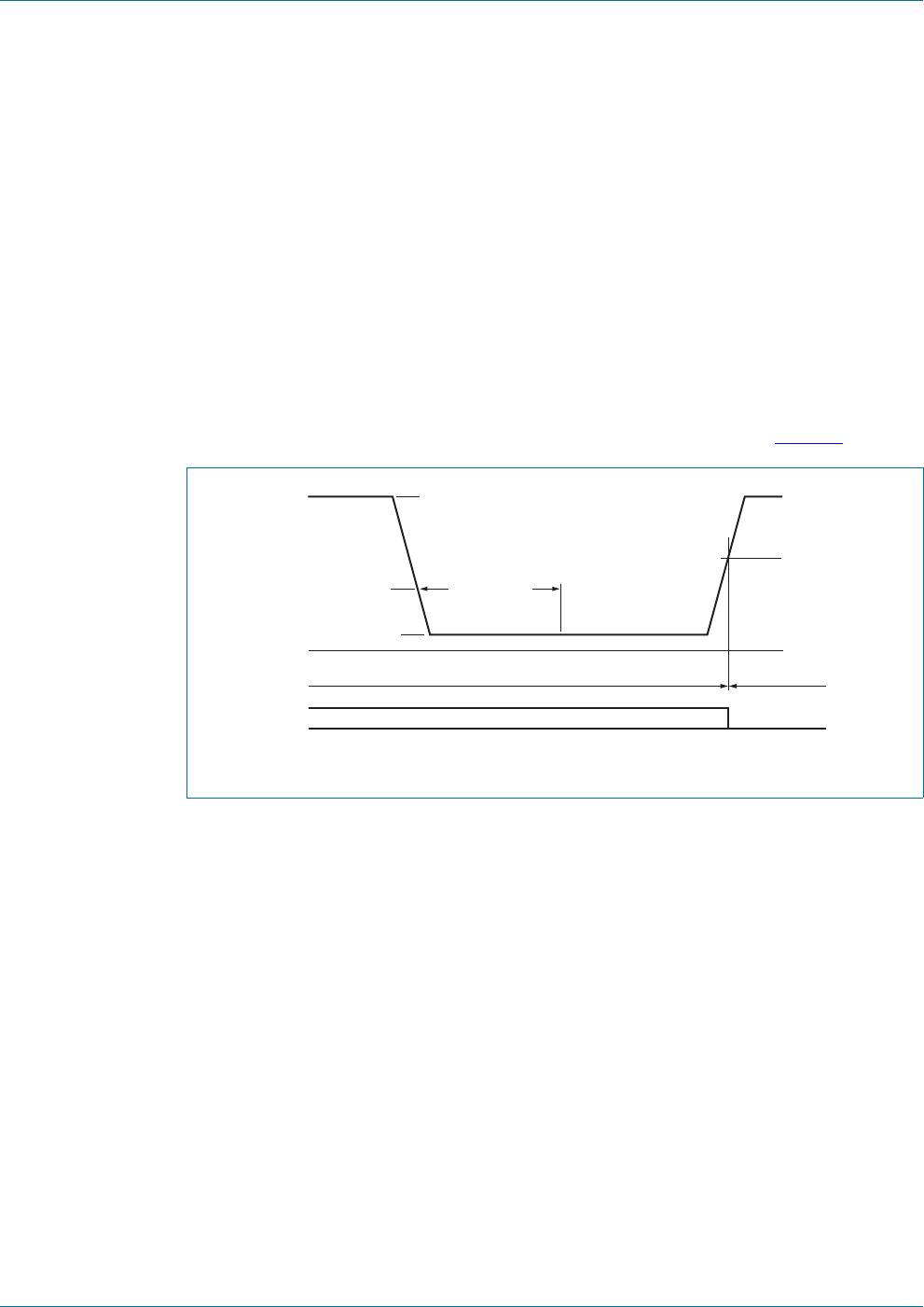
7.6.2 TXD dominant time-out function
A TXD dominant time-out timer circuit prevents the bus line being driven to a permanent
dominant state (blocking all network communications) if TXD is forced permanently LOW
by a hardware or software application failure. The timer is triggered by a negative edge on
the TXD pin. If the pin remains LOW for longer than the TXD dominant time-out time
(t
to(dom)TXD
), the transmitter is disabled, driving the bus line to a recessive state. The timer
is reset by a positive edge on TXD.
7.6.3 Temperature protection
The temperature of the IC is monitored in Normal, Standby and Off modes. If the
temperature is too high (T
vj
>T
th(act)otp
), the TJA1028 will switch to Off mode (if in Standby
or Normal modes). The voltage regulator and the LIN transmitter will be switched off and
the RSTN pin driven LOW.
When the temperature falls below the overtemperature protection release threshold
(T
vj
<T
th(rel)otp
), the TJA1028 switches to Standby mode.
8. Limiting values
[1] Human Body Model (HBM): according to AEC-Q100-002 (100 pF, 1.5 k).
[2] V
CC
and V
BAT
connected to GND, emulating application circuit.
Table 4. Limiting values
In accordance with the Absolute Maximum Rating System (IEC 60134).
Symbol Parameter Conditions Min Max Unit
V
BAT
battery supply voltage DC; continuous 0.3 +40 V
V
x
voltage on pin x DC value
pin V
CC
0.3 +7 V
pins TXD, RXD, RSTN and EN 0.3 V
CC
+0.3 V
pin LIN with respect to GND 40 +40 V
V
ESD
electrostatic discharge
voltage
HBM
[1]
at pins LIN and V
BAT
[2]
8+8 kV
at any other pin 2+2 kV
IEC 61000-4-2
[3]
at pins LIN and V
BAT
8+8 kV
MM
[4]
at any pin 250 +250 V
CDM
[5]
at corner pins 750 +750 V
at any other pin 500 +500 V
V
trt
transient voltage on pin V
BAT
via reverse polarity diode/capacitor;
on pin LIN via 1 nF coupling capacitor
[6]
150 +100 V
T
vj
virtual junction temperature
[7]
40 +150 C
T
stg
storage temperature 55 +150 C

TJA1028T/5V0/10,11

Mfr. #:
Manufacturer:
NXP Semiconductors
Description:
LIN Transceivers 5V 850uA 6us
Lifecycle:
New from this manufacturer.
Delivery:
DHL FedEx Ups TNT EMS
Payment:
T/T Paypal Visa MoneyGram Western Union