MP1470 – SYNCHRONOUS, STEP-DOWN CONVERTER WITH INTERNAL MOSFETS
MP1470 Rev. 1.02 www.MonolithicPower.com 10
8/27/2013 MPS Proprietary Information. Patent Protected. Unauthorized Photocopy and Duplication Prohibited.
© 2013 MPS. All Rights Reserved.
resistor to the V
IN
voltage limits the EN input
current to less than 100A.
For example, with 12V connected to Vin,
R
PULLUP
(12V-6.5V) ÷100A =55k
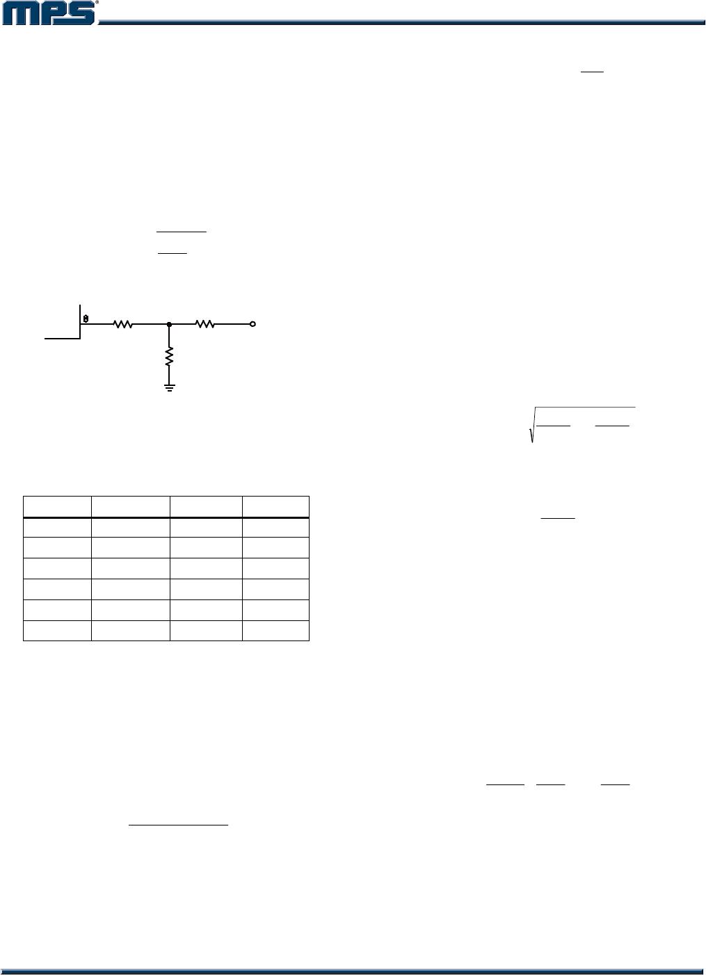
Connecting the EN pin directly to a voltage
source without any pullup resistor requires
limiting the amplitude of the voltage source to
6V to prevent damage to the Zener diode.
EN LOGIC
EN
GND
Zener
6.5V-typ
Figure 4: 6.5V Zener Diode
Under-Voltage Lockout (UVLO)
Under-voltage lockout (UVLO) protects the chip
from operating at an insufficient supply voltage.
The MP1470 UVLO comparator monitors the
output voltage of the internal regulator, VCC.
The UVLO rising threshold is about 4.2V while
its falling threshold is consistently 3.85V.
Internal Soft-Start
Soft-start prevents the converter output voltage
from overshooting during startup. When the
chip starts, the internal circuit generates a soft-
start voltage (SS) that ramps up from 0V to
1.2V: When SS falls below the internal
reference (REF), SS overrides REF so that the
error amplifier uses SS as the reference; when
SS exceeds REF, the error amplifier resumes
using REF as its reference. The SS time is
internally set to 1ms.
Over-Current-Protection and Hiccup
The MP1470 has a cycle-by-cycle over-current
limit for when the inductor current peak value
exceeds the set current-limit threshold. First,
when the output voltage drops until FB falls
below the Under-Voltage (UV) threshold
(typically 140mV) to trigger a UV event, the
MP1470 enters hiccup mode to periodically
restart the part. This protection mode is
especially useful when the output is dead-
shorted to ground. This greatly reduces the
average short-circuit current to alleviate thermal
issues and to protect the regulator. The
MP1470 exits hiccup mode once the over-
current condition is removed.
Thermal Shutdown
Thermal shutdown prevents the chip from
operating at exceedingly high temperatures.
When the silicon die temperature exceeds
150°C, it shuts down the whole chip. When the
temperature falls below its lower threshold
(typically 130°C) the chip is enabled again.
Floating Driver and Bootstrap Charging
An external bootstrap capacitor powers the
floating power MOSFET driver. This floating
driver has its own UVLO protection, with a
rising threshold of 2.2V and a hysteresis of
150mV. V
IN
regulates the bootstrap capacitor
voltage internally through D1, M1, R4, C4, L1
and C2 (Figure 5). If (V
IN
-V
SW
) exceeds 5V, U2
will regulate M1 to maintain a 5V BST voltage
across C4.
U2
V
IN
U1
5V
D1
M1
R4
C4
SW
L1
C2
V
OUT
Figure 5: Internal Bootstrap Charger Start-Up
and Shutdown Circuit
If both V
IN
and EN exceed their respective
thresholds, the chip starts. The reference block
starts first, generating stable reference voltage
and currents, and then the internal regulator is
enabled. The regulator provides a stable supply
for the remaining circuits.
Three events can shut down the chip: EN low,
V
IN
low, and thermal shutdown. The shutdown
procedure starts by initially blocking the
signaling path to avoid any fault triggering. The
COMP voltage and the internal supply rail are
then pulled down. The floating driver is not
subject to this shutdown command.
MP1470 – SYNCHRONOUS, STEP-DOWN CONVERTER WITH INTERNAL MOSFETS
MP1470 Rev. 1.02 www.MonolithicPower.com 11
8/27/2013 MPS Proprietary Information. Patent Protected. Unauthorized Photocopy and Duplication Prohibited.
© 2013 MPS. All Rights Reserved.
APPLICATION INFORMATION
Setting the Output Voltage
The external resistor divider sets the output
voltage. The feedback resistor R1 also sets the
feedback-loop bandwidth through the internal
compensation capacitor (see the Typical
Application circuit). Choose R1 around 10k,
and R2with:
OUT
R1
R2
V
1
0.8V
=
Use a T-type network for when V
OUT
is low.
FB
VOUT
R1RT
R2
Figure 6: T-Type Network
Table 1 lists the recommended T-type resistors
value for common output voltages.
Table 1: Resistor Selection for Common Output
Voltages
V
OUT
(V) R1 (k) R2 (k) Rt (k)
1.05 10(1%) 32.4(1%) 300(1%)
1.2 20.5(1%) 41.2(1%) 249(1%)
1.8 40.2(1%) 32.4(1%) 120(1%)
2.5 40.2(1%) 19.1(1%) 100(1%)
3.3 40.2(1%) 13(1%) 75(1%)
5 40.2(1%) 7.68(1%) 75(1%)
Selecting the Inductor
Use a 1µH-to-10µH inductor with a DC current
rating of at least 25% percent higher than the
maximum load current for most applications.
For highest efficiency, select an inductor with a
DC resistance less than 15m. For most
designs, derive the inductance value from the
following equation.
OUT IN OUT
1
IN L OSC
V(VV)
L
VIf
×−
=
×Δ ×
Where I
L
is the inductor ripple current. Choose
an inductor current approximately 30% of the
maximum load current. The maximum inductor
peak current is:
2
I
II
L
LOAD)MAX(L
Δ
+=
Under light-load conditions (below 100mA), use
a larger inductor to improve efficiency.
Selecting the Input Capacitor
The input current to the step-down converter is
discontinuous, and therefore requires a
capacitor to both supply the AC current to the
step-down converter and maintain the DC input
voltage. For the best performance, use low
ESR capacitors, such as ceramic capacitors
with X5R or X7R dielectrics and small
temperature coefficients. A 22µF capacitor is
sufficient for most applications.
The input capacitor (C1) requires an adequate
ripple current rating because it absorbs the
input switching. Estimate the RMS current in
the input capacitor with:
×
×=
IN
OUT
IN
OUT
LOAD1C
V
V
1
V
V
II
The worst-case condition occurs at V
IN
= 2V
OUT
,
where:
2
I
I
LOAD
1C
=
For simplification, choose an input capacitor
with an RMS current rating greater than half the
maximum load current.
The input capacitor can be electrolytic, tantalum,
or ceramic. Place a small, high-quality, ceramic
capacitor (0.1F) as close to the IC as possible
when using electrolytic or tantalum capacitors.
When using ceramic capacitors, make sure that
they have enough capacitance to provide
sufficient charge to prevent excessive input
voltage ripple. Estimate the input voltage ripple
caused by the capacitance with:
LOAD OUT OUT
IN
IN
SIN
IV V
V1
fC1V V
⎛⎞
Δ= × ×
⎜⎟
×
⎝⎠
Selecting the Output Capacitor
The output capacitor (C2) maintains the DC
output voltage. Use ceramic, tantalum, or low-
ESR electrolytic capacitors. Use low ESR
capacitors to limit the output voltage ripple.
Estimate the output voltage ripple with:
MP1470 – SYNCHRONOUS, STEP-DOWN CONVERTER WITH INTERNAL MOSFETS
MP1470 Rev. 1.02 www.MonolithicPower.com 12
8/27/2013 MPS Proprietary Information. Patent Protected. Unauthorized Photocopy and Duplication Prohibited.
© 2013 MPS. All Rights Reserved.
OUT OUT
OUT ESR
S1 IN S
VV
1
V1R
fL V 8fC2
⎛⎞
⎛⎞
Δ= × × +
⎜⎟
⎜⎟
×××
⎝⎠
⎝⎠
Where L
1
is the inductor value and R
ESR
is the
equivalent series resistance (ESR) of the output
capacitor.
For ceramic capacitors, the capacitance
dominates the impedance at the switching
frequency and causes most of the output
voltage ripple. For simplification, estimate the
output voltage ripple with:
OUT OUT
OUT
2
IN
S1
VV
V1
V
8f L C2
⎛⎞
⎜⎟
×××
⎝⎠
For tantalum or electrolytic capacitors, the ESR
dominates the impedance at the switching
frequency. For simplification, the output ripple
can be approximated with:
OUT OUT
OUT ESR
IN
S1
VV
V1R
fL V
⎛⎞
×
⎜⎟
×
⎝⎠
The characteristics of the output capacitor also
affect the stability of the regulation system. The
MP1470 can be optimized for a wide range of
capacitance and ESR values.
External Bootstrap Diode
An external bootstrap (BST) diode can enhance
the efficiency of the regulator given the
following applicable conditions:
z V
OUT
is 5V or 3.3V; and
z Duty cycle is high: D=
IN
OUT
V
V
>65%
Connect the external BST diode from the output
of voltage regulator to the BST pin, as shown in
Figure 7
MP1470
SW
C
OUT
L
5V or 3.3V
R4
External BST Diode
IN4148
BST
Figure 7: Optional External Bootstrap Diode
For most applications, use an IN4148 for the
external BST diode is IN4148, and a 1µF
capacitor for the BST capacitor.
PC BOARD LAYOUT
PCB layout is very important to achieve stable
operation. For best results, use the following
guidelines and Figure 8 as reference.
1) Keep the connection between the input
ground and GND pin as short and wide as
possible.
2) Keep the connection between the input
capacitor and IN pin as short and wide as
possible.
3) Use short and direct feedback connections.
Place the feedback resistors and compensation
components as close to the chip as possible.
4) Route SW away from sensitive analog areas
such as FB.
C1
C6
C2
L1
R1
R2
R7
R6 C5
R4
C3
R5
123
456
VIN
GND
V
OUT
C2A
C3
R3
C1
C1A
C6
C2
C2 A
L1
R8
R1
R2
R7
C7
R3
C3
R6 C5
R4
C4
R5
1
23
456
VIN
GND
Figure 8: Sample Board Layout

MP1470GJ-Z

Mfr. #:
Manufacturer:
Monolithic Power Systems (MPS)
Description:
Switching Voltage Regulators 2A, 16V, 500kHz Sync, Stp-Dwn Cnvrtr
Lifecycle:
New from this manufacturer.
Delivery:
DHL FedEx Ups TNT EMS
Payment:
T/T Paypal Visa MoneyGram Western Union

Products related to this Datasheet