1©2015 Integrated Device Technology, Inc. Revision C, December 8, 2015
General Description
The 8545 is a low skew, high performance 1-to-4
LVCMOS/LVTTL-to-LVDS Clock Fanout Buffer. Utilizing Low Voltage
Differential Signaling (LVDS) the 8545 provides a low power, low
noise, solution for distributing clock signals over controlled
impedances of 100. The 8545 accepts a LVCMOS/LVTTL input
level and translates it to 3.3V LVDS output levels.
Guaranteed output and part-to-part skew characteristics make the
8545 ideal for those applications demanding well defined
performance and repeatability.
Features
Four differential LVDS output pairs
Two LVCMOS/LVTTL clock inputs to support redundant
or selectable frequency fanout applications
Maximum output frequency: 650MHz
Translates LVCMOS/LVTTL input signals to LVDS levels
Output skew: 40ps (maximum)
Part-to-part skew: 500ps (maximum)
Propagation delay: 3.6ns (maximum)
Additive phase jitter, RMS: 0.13ps (typical)
Full 3.3Vsupply mode
-40°C to 85°C ambient operating temperature
Available in lead-free (RoHS 6) package
8545
20-Lead TSSOP
6.5mm x 4.4mm x 0.925mm package body
G Package
Top View
Pin Assignment
Block Diagram
0
1
nD
Q
LE
0
1
Q0
Q0
Q1
Q1
Q2
Q2
Q3
Q3
CLK_EN
CLK1
CLK2
CLK_SEL
OE
Pulldown
Pulldown
Pulldown
Pullup
Pullup
1
2
3
4
5
6
7
8
9
10
20
19
18
17
16
15
14
13
12
11
GND
OE
nc
CLK2
nc
CLK1
CLK_SEL
CLK_EN
GND
V
DD
Q0
Q0
V
DD
Q1
Q1
Q2
Q2
GND
Q3
Q3
8545
Datasheet
Low Skew, 1-to-4 LVCMOS/ LVTTL-to-LVDS
Fanout Buffer
2©2015 Integrated Device Technology, Inc. Revision C, December 8, 2015
8545 Datasheet
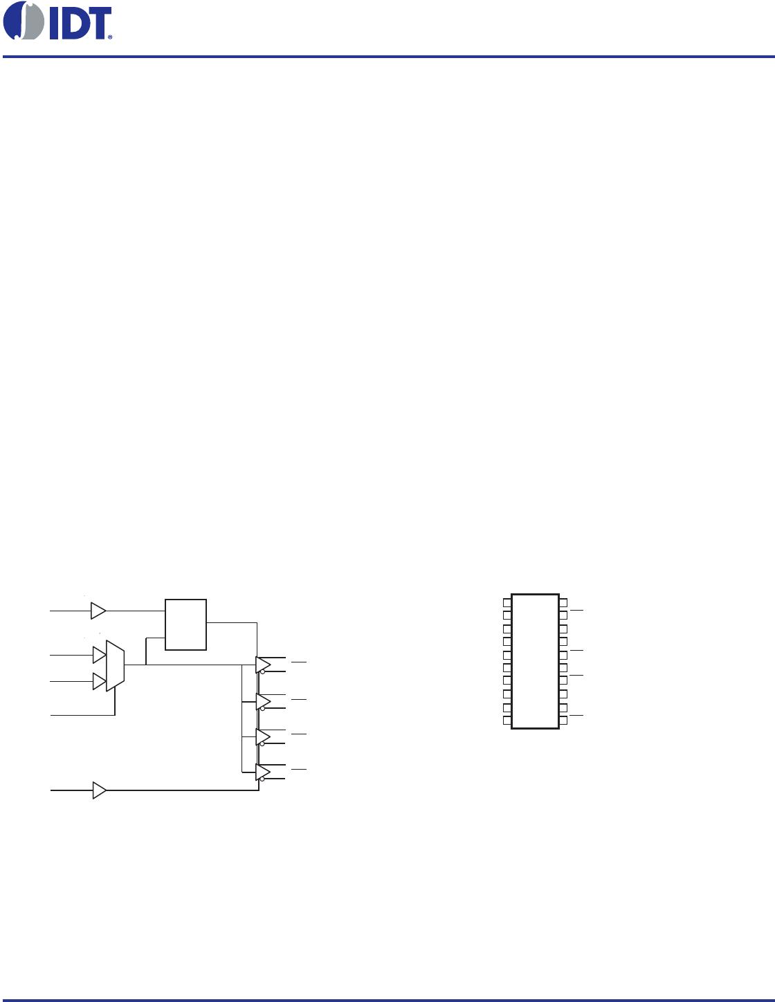
Pin Description and Pin Characteristic Tables
Table 1. Pin Descriptions
NOTE: Pullup and Pulldown refer to internal input resistors. See Table 2, Pin Characteristics, for typical values.
Table 2. Pin Characteristics
Number Name Type Description
1, 9, 13 GND Power Power supply ground.
2 CLK_EN Input Pullup
Synchronizing clock enable. When HIGH, clock outputs follows clock input.
When LOW, Q outputs are forced low, Q
outputs are forced high.
LVCMOS / LVTTL interface levels.
3 CLK_SEL Input Pulldown
Clock select input. When HIGH, selects CLK2 input.
When LOW, selects CLK1 input. LVCMOS / LVTTL interface levels.
4 CLK1 Input Pulldown Single-ended clock input. LVCMOS/LVTTL interface levels.
5, 7 nc Unused No connect.
6 CLK2 Input Pulldown Single-ended clock input. LVCMOS/LVTTL interface levels.
8 OE Input Pullup
Output enable. Controls enabling and disabling of outputs Q0/Q0
through
Q3/Q3
. LVCMOS/LVTTL interface levels.
10, 18 V
DD
Power Positive supply pins.
11, 12 Q3
, Q3 Output Differential output pair. LVDS interface levels.
14, 15 Q2
, Q2 Output Differential output pair. LVDS interface levels.
16, 17 Q1
, Q1 Output Differential output pair. LVDS interface levels.
19, 20 Q0
, Q0 Output Differential output pair. LVDS interface levels.
Symbol Parameter Test Conditions Minimum Typical Maximum Units
C
IN
Input Capacitance 4 pF
R
PULLUP
Input Pullup Resistor 51 k
R
PULLDOWN
Input Pulldown Resistor 51 k
3©2015 Integrated Device Technology, Inc. Revision C, December 8, 2015
8545 Datasheet
Function Tables
Table 3A. Control Input Function Table
After CLK_EN switches, the clock outputs are disabled or enabled following a rising and falling input clock edge as shown in Figure 1.
In the active mode, the state of the outputs are a function of the CLK1 and CLK2 inputs as described in Table 3B.
Figure 1. CLK_EN Timing Diagram
Table 3B. Clock Input Function Table
Inputs Outputs
OE CLK_EN CLK_SEL Selected Source Q0:Q3 Q0
:Q3
0 X X Hi-Z Hi-Z
1 0 0 CLK1 Low High
1 0 1 CLK2 Low High
1 1 0 CLK1 Active Active
1 1 1 CLK2 Active Active
Inputs Outputs
CLK1 or CLK2 Q0:Q3 Q0
:Q3
0LOWHIGH
1HIGHLOW
Enabled
Disabled
CLK1, CLK2
CLK_EN
Q0
:Q3
Q0:Q3

8545BGILF

Mfr. #:
Manufacturer:
IDT
Description:
Clock Buffer 1-to-4 LVCMOS/LVTTL- to-LVDS Fanout Buffe
Lifecycle:
New from this manufacturer.
Delivery:
DHL FedEx Ups TNT EMS
Payment:
T/T Paypal Visa MoneyGram Western Union

Products related to this Datasheet