10©2015 Integrated Device Technology, Inc. Revision C, December 8, 2015
8545 Datasheet
Applications Information
Recommendations for Unused Input and Output Pins
Inputs:
CLK Inputs
For applications not requiring the use of a clock input, it can be left
floating. Though not required, but for additional protection, a 1k
resistor can be tied from the CLK input to ground.
LVCMOS Control Pins
All control pins have internal pull-ups or pull-downs; additional
resistance is not required but can be added for additional protection.
A 1k resistor can be used.
Outputs:
LVDS O ut p ut s
All unused LVDS output pairs can be either left floating or terminated
with 100 across. If they are left floating, there should be no trace
attached.
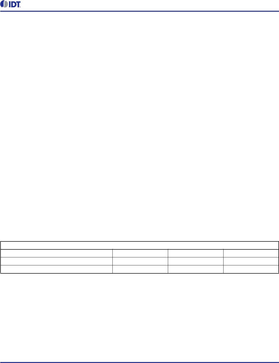
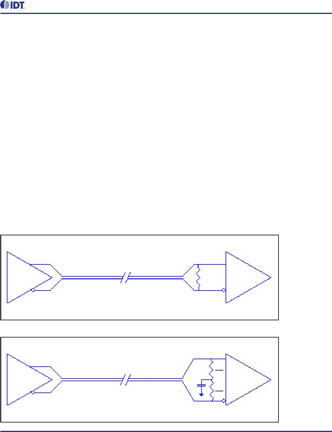
LVDS Driver Termination
For a general LVDS interface, the recommended value for the
termination impedance (Z
T
) is between 90 and 132. The actual
value should be selected to match the differential impedance (Z
0
) of
your transmission line. A typical point-to-point LVDS design uses a
100 parallel resistor at the receiver and a 100 differential
transmission-line environment. In order to avoid any
transmission-line reflection issues, the components should be
surface mounted and must be placed as close to the receiver as
possible. IDT offers a full line of LVDS compliant devices with two
types of output structures: current source and voltage source. The
standard termination schematic as shown in Figure 2 can be used
with either type of output structure. Figure 3, which can also be used
with both output types, is an optional termination with center tap
capacitance to help filter common mode noise. The capacitor value
should be approximately 50pF. If using a non-standard termination,
it is recommended to contact IDT and confirm if the output structure
is current source or voltage source type. In addition, since these
outputs are LVDS compatible, the input receiver’s amplitude and
common-mode input range should be verified for compatibility with
the output.
Figure 2. Standard LVDS Termination
Figure 3. Optional LVDS Termination
LVDS
Driver
Z
O
Z
T
Z
T
LVD S
Receiver
LVD S
Driver
Z
O
Z
T
LVD S
Receiver
C
Z
T
2
Z
T
2