4©2015 Integrated Device Technology, Inc. Revision C, December 8, 2015
8545 Datasheet
Absolute Maximum Ratings
NOTE: Stresses beyond those listed under Absolute Maximum Ratings may cause permanent damage to the device.
These ratings are stress specifications only. Functional operation of product at these conditions or any conditions beyond
those listed in the DC Characteristics or AC Characteristics is not implied. Exposure to absolute maximum rating conditions for
extended periods may affect product reliability.
DC Electrical Characteristics
Table 4A. Power Supply DC Characteristics, V
DD
= 3.3V ± 5%, T
A
= -40°C to 85°C
Table 4B. LVCMOS/LVTTL DC Characteristics, V
DD
= 3.3V ± 5%, T
A
= -40°C to 85°C
Item Rating
Supply Voltage, V
DD
4.6V
Inputs, V
I
-0.5V to V
DD
+ 0.5V
Outputs, I
O
Continuous Current
Surge Current
10mA
15mA
Package Thermal Impedance,
JA
73.2C/W (0 lfpm)
Storage Temperature, T
STG
-65C to 150C
Symbol Parameter Test Conditions Minimum Typical Maximum Units
V
DD
Positive Supply Voltage 3.135 3.3 3.465 V
I
DD
Power Supply Current 52 mA
Symbol Parameter Test Conditions Minimum Typical Maximum Units
V
IH
Input High Voltage 2 V
DD
+ 0.3 V
V
IL
Input
Low Voltage
CLK1, CLK2 -0.3 1.3 V
OE, CLK_EN, CLK_SEL -0.3 0.8 V
I
IH
Input
High Current
CLK1, CLK2, CLK_SEL V
DD
= V
IN
= 3.465V 150 µA
OE, CLK_EN V
DD
= V
IN
= 3.465V 5 µA
I
IL
Input
Low Current
CLK1, CLK2, CLK_SEL V
DD
= 3.465V, V
IN
= 0V -5 µA
OE, CLK_EN V
DD
= 3.465V, V
IN
= 0V -150 µA
5©2015 Integrated Device Technology, Inc. Revision C, December 8, 2015
8545 Datasheet
Table 4C. LVDS DC Characteristics, V
DD
= 3.3V ± 5%, T
A
= -40°C to 85°C
AC Electrical Characteristics
Table 5. AC Characteristics, V
DD
= 3.3V ± 5%, T
A
= -40°C to 85°C
All parameters measured at ƒ 650MHz unless noted otherwise.
NOTE 1: Measured from V
DD
/2 of the input to the differential output crossing point.
NOTE 2: Defined as skew between outputs at the same supply voltage and with equal load conditions.
Measured at V
DD
/2 of the input to the differential output crossing point.
NOTE 3: Defined as skew between outputs on different devices operating at the same supply voltages and with equal load conditions.
Using the same type of inputs on each device, the outputs are measured at the differential cross points.
NOTE 4: This parameter is defined in accordance with JEDEC Standard 65.
Symbol Parameter Test Conditions Minimum Typical Maximum Units
V
OD
Differential Output Voltage 200 280 360 mV
V
OD
V
OD
Magnitude Change 40 mV
V
OS
Offset Voltage 1.125 1.25 1.375 V
V
OS
V
OS
Magnitude Change 5 25 mV
I
Oz
High Impedance Leakage -10 ±1 +10 µA
I
OFF
Power Off Leakage -20 ±1 +20 µA
I
OSD
Differential Output Short Circuit Current -3.5 -5 mA
I
OS
Output Short Circuit Current -3.5 -5 mA
V
OH
Output Voltage High 1.34 1.6 V
V
OL
Output Voltage Low 0.9 1.06 V
Symbol Parameter Test Conditions Minimum Typical Maximum Units
f
MAX
Output Frequency 650 MHz
t
PD
Propagation Delay; NOTE 1 ƒ 650MHz 1.4 3.6 ns
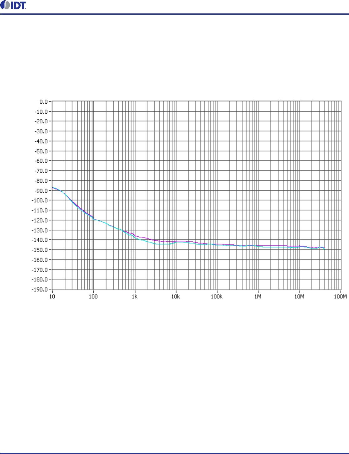
tjit
Buffer Additive Phase Jitter, RMS;
refer to Additive Phase Jitter Section
156.25MHz, Integration
Range: 12kHz – 20MHz
0.13 ps
tsk(o) Output Skew; NOTE 2, 4 40 ps
tsk(pp) Part-to-Part Skew; NOTE 3, 4 500 ps
t
R
/ t
F
Output Rise/Fall Time 20% to 80% @ 50MHz 200 400 700 ps
odc Output Duty Cycle
ƒ 266MHz 45 55 %
ƒ > 266MHz 40 60 %
6©2015 Integrated Device Technology, Inc. Revision C, December 8, 2015
8545 Datasheet
Additive Phase Jitter
The spectral purity in a band at a specific offset from the fundamental
compared to the power of the fundamental is called the dBc Phase
Noise. This value is normally expressed using a Phase noise plot
and is most often the specified plot in many applications. Phase noise
is defined as the ratio of the noise power present in a 1Hz band at a
specified offset from the fundamental frequency to the power value of
the fundamental. This ratio is expressed in decibels (dBm) or a ratio
of the power in the 1Hz band to the power in the fundamental. When
the required offset is specified, the phase noise is called a dBc value,
which simply means dBm at a specified offset from the fundamental.
By investigating jitter in the frequency domain, we get a better
understanding of its effects on the desired application over the entire
time record of the signal. It is mathematically possible to calculate an
expected bit error rate given a phase noise plot.
As with most timing specifications, phase noise measurements have
issues. The primary issue relates to the limitations of the equipment.
Often the noise floor of the equipment is higher than the noise floor
of the device. This is illustrated above. The device meets the noise
floor of what is shown, but can actually be lower. The phase noise is
dependent on the input source and measurement equipment.
SSB Phase Noise dBc/Hz
Offset Frequency (Hz)

8545BGILF

Mfr. #:
Manufacturer:
IDT
Description:
Clock Buffer 1-to-4 LVCMOS/LVTTL- to-LVDS Fanout Buffe
Lifecycle:
New from this manufacturer.
Delivery:
DHL FedEx Ups TNT EMS
Payment:
T/T Paypal Visa MoneyGram Western Union

Products related to this Datasheet