10
LTC1479
OPERATION
U
The LTC1479 is responsible for low-loss switching at the
“front end” of the power management system, where up
to two battery packs and a DC power source can be
indiscriminately connected and disconnected. Smooth
switching between input power sources is accomplished
with the help of low-loss N-channel switches driven by
special gate drive circuitry which limits the inrush current
in and out of the battery packs and the system power
supply capacitors.
All N-Channel Switching
The LTC1479 drives external back-to-back N-channel
MOSFET switches to direct power from the three main
power sources: the external DC power source, the pri-
mary battery and the secondary battery connected to the
main supply pinsDCIN, BAT1 and BAT2 respectively.
(N-channel MOSFET switches are more cost effective
and provide lower voltage drops than their P-channel
counterparts.)
Gate Drive (V
GG
) Power Supply
The gate drive for the low-loss N-channel switches is
supplied by a micropower boost regulator which is regu-
lated at approximately 36.5V. The V
GG
supply provides
sufficient headroom above the maximum 28V operating
voltage of the three main power sources to ensure that the
MOSFET switches are fully enhanced.
The power for this inductor based regulator is taken from
three internal diodes as shown in Figure 1. The three
Figure 1. V
GG
Switching Regulator
BAT1
BAT2
DCIN
V
+
SW
GND
1479 F01
V
GG
+
+
L1
1mH
C1
1µF
35V
C2
1µF
50V
TO GATE
DRIVERS
(36.5V)
LTC1479
V
GG
SWITCHING
REGULATOR
diodes are connected to each of the three main power
sources, DCIN, BAT1 and BAT2. The highest voltage
potential is directed to the top of the boost regulator
inductor to maximize regulator efficiency. C1 provides
filtering at the top of the 1mH switched inductor, L1, which
is housed in a small surface mount package.
A fourth internal diode directs the current from the 1mH
inductor to the V
GG
output capacitor, C2, further reducing
the external parts count. In fact, as demonstrated in Figure
1, only three external components are required by the V
GG
regulator, L1, C1 and C2.
Inrush Current Limiting
The LTC1479 uses an adaptive inrush current limiting
scheme to reduce current flowing in and out of the three
main power sources and the DC/DC converter input ca-
pacitor during switch-over transitions. The voltage across
a single small-valued resistor, R
SENSE
, is measured to
ascertain the instantaneous current flowing through the
three main switch pairs, SW A/B, SW C/D, and SW E/F
during the transitions.
Figure 2 is a block diagram showing only the DCIN switch
pair, SW A/B. (The gate drive circuits for switch pairs SW
C/D and SW E/F are identical). A bidirectional current
sensing and limiting circuit determines when the voltage
drop across R
SENSE
reaches plus or minus 200mV. The
gate-to-source voltage, V
GS
, of the appropriate switch is
limited during the transition period until the inrush current
subsides, generally within a few milliseconds, depending
upon the value of the DC/DC converter input capacitor.
V
SENSE
+
V
SENSE
GA GBSAB
SW A SW B R
SENSE
V
GG
LTC1479
1479 F02
DCIN
+
OUTPUT
TO DC/DC
CONVERTER
C
OUT
6V 6V
±200mV
THRESHOLD
SW A/B
GATE
DRIVERS
BIDIRECTIONAL
INRUSH CURRENT
SENSING AND
LIMITING
Figure 2. SW A/B Inrush Current Limiting
11
LTC1479
OPERATION
U
This scheme allows capacitors and MOSFET switches of
differing sizes and current ratings to be used in the same
system without circuit modifications.
After the transition period has passed, the V
GS
of both
MOSFETs in the selected switch pair rises to approxi-
mately 6V. The gate drive is set at 6V to provide ample
overdrive for logic level MOSFET switches without ex-
ceeding their maximum V
GS
rating.
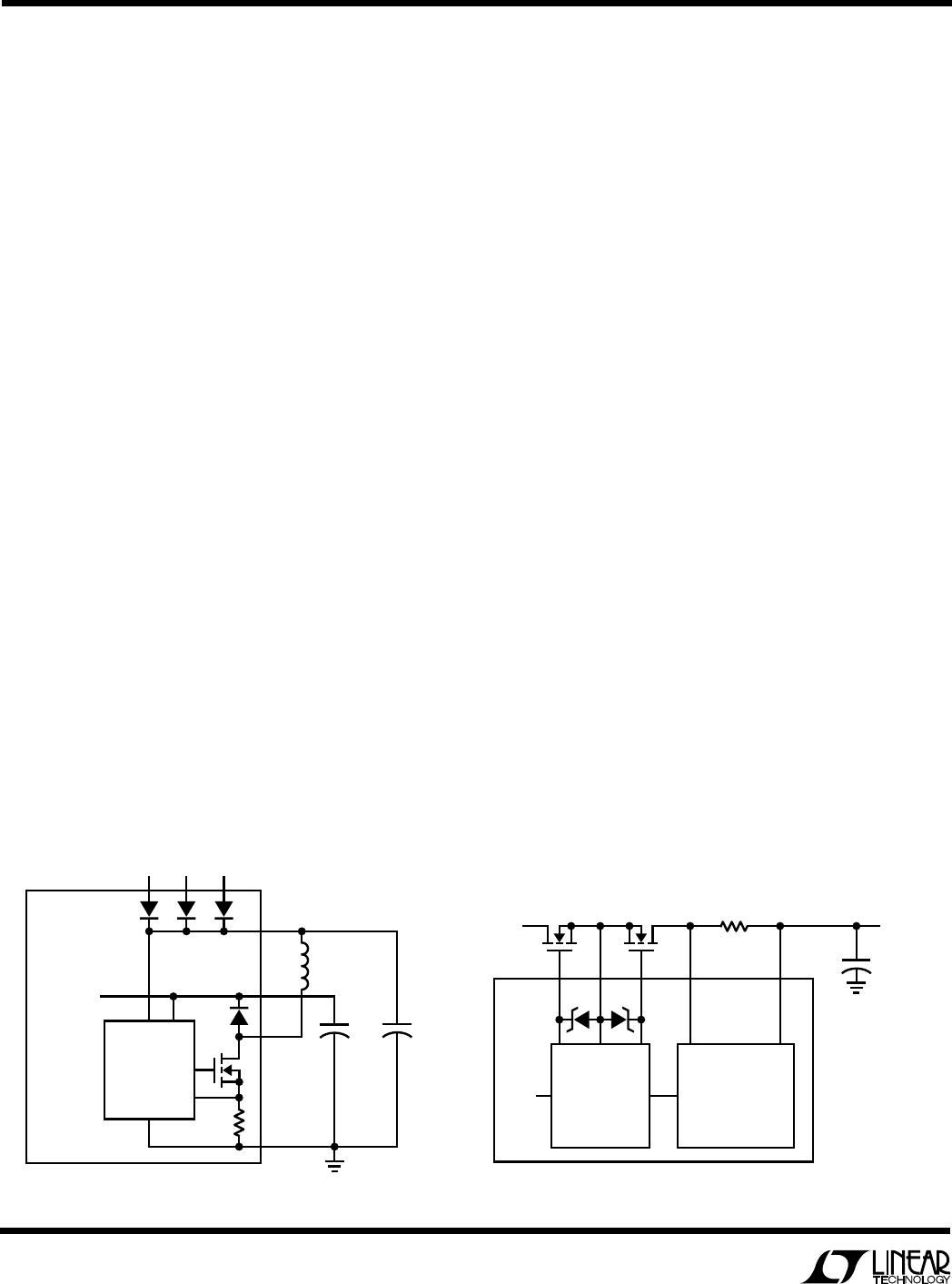
Internal Power Supplies
Two internal supplies provide power for the control logic
and power source monitoring functions. The V
CCP
logic
supply is approximately 5V and provides power for the
majority of the internal logic circuitry. The V
CC
supply is
approximately 3.60V and provides power for the V
GG
switching regulator control circuitry and the gate drivers.
The V
CC
supply has an undervoltage lockout circuit which
minimizes power consumption in the event of a total loss
of system power; i.e., when all available power sources fall
below approximately 4.5V.
DCIN Voltage Monitoring
The DCIN input is continuously monitored via a two
resistor ladder connected between the DCIN pin and the
DCDIV input. The input threshold is 1.215V (rising edge)
with approximately –35mV hysteresis. The use of a defini-
tive voltage threshold ensures that the DC supply is not
only connected but “healthy” before being attached to the
DC/DC converter input.
Battery Voltage Monitoring
The LTC1479 has the ability to independently monitor both
battery packs. (Because of this, one battery pack may be
discharged as the other is being charged.)
A low-battery detector signals when the selected battery
pack has dropped to the level where a shutdown sequence
should be initiated or the other battery pack engaged.
Battery Charging Management Functions
The LTC1479 directly interfaces with LT1510/LT1511
battery charger circuits. Two gate drive circuits control
the two back-to-back N-channel switch pairs, SW G and
SW H, under logic (CHGSEL) control to connect the
output of the charger to the selected battery pack. Break-
before-make action ensures that current does not pass
from one battery pack to the other during switch-over of
the charger output. The CHGSEL input also simulta-
neously switches the positive terminal of the selected
battery pack to the top of the voltage feedback resistor
ladder in the charger system through the CHGMON pin.
Backup Supply Interface
Power for the LTC1479 is obtained from the backup
supply when power is unavailable from the three main
sources of power.
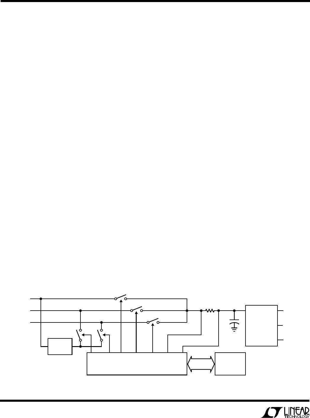
Interface to Companion Microprocessor
A companion µP must be used in conjunction with the
LTC1479 to provide overall control of the power manage-
ment system. The LTC1479 communicates with the µP by
means of five logic inputs and two logic outputs as
described in Table 1.
Table 1. LTC1479 µP Interface Inputs and Outputs
INPUT ACTION
DCIN/BAT Logic High Required to Connect a Good DC Supply
BATDIS Logic Low Disconnects the Battery from the System
BATSEL Selects Which Battery is Connected to the System
(Logic High Selects BAT1; Logic Low Selects BAT2)
CHGSEL Selects Which Battery is Charged and Monitored
(Logic High Selects BAT1; Logic Low Selects BAT2)
3DM Forces the Main Three Power Path Switches Into
“3-Diode Mode.” See Applications Information Section
OUTPUT ACTION
DCINGOOD Logic High When a Good DC Supply is Present
LOBAT Logic Low When Selected Battery Voltage is Low
12
LTC1479
APPLICATIONS INFORMATION
WUU
U
POWER PATH SWITCHING CONCEPTS
Power Source Selection
The LTC1479 drives low-loss switches to direct power in
the main power path of a dual rechargeable battery system
— the type found in most notebook computers and other
portable equipment.
Figure 3 is a conceptual block diagram which illustrates
the main features of an LTC1479 dual battery power
management system, starting with the three main power
sources and ending at the system DC/DC regulator.
Switches SW A/B, SW C/D and SW E/F direct power from
either the AC adapter (DCIN) or one of the two battery
packs (BAT1 and BAT2) to the input of the DC/DC switch-
ing regulator. Switches SW G and SW H connect the
desired battery pack to the battery charger.
Each of the five switches is intelligently controlled by the
LTC1479 which interfaces directly with a power manage-
ment system µP.
Using Tantalum Capacitors
The inrush and “outrush” current of the system DC/DC
regulator input capacitor is limited by the LTC1479. i.e.,
the current flowing both in and out of the capacitor during
transitions from one input power source to another is
limited. In many applications, this inrush current limiting
makes it feasible to use lower cost/size tantalum surface
mount capacitors in place of more expensive/larger alumi-
num electrolytics at the input of the DC/DC converter.
Note: The capacitor manufacturer should be consulted for
specific inrush current specifications and limitations and
some experimentation may be required to ensure compli-
ance with these limitations under all possible operating
conditions.
Back-to-Back Switch Topology
The simple SPST switches shown in Figure 3 actually
consist of two back-to-back N-channel switches. These
low-loss, N-channel switch pairs are housed in 8-pin SO
and SSOP packaging and are available from a number of
manufacturers. The back-to-back topology eliminates the
problems associated with the inherent body diodes in
power MOSFET switches and allows each switch pair to
block current flow in either direction when the two switches
are turned off.
The back-to-back topology also allows for independent
control of each half of the switch pair which facilitates
bidirectional inrush current limiting and the so called “3-
diode” mode described in the following section.
The “3-Diode” Mode
Under normal operating conditions, both halves of each
switch pair are turned on and off simultaneously. For
example, when the input power source is switched from a
good DC input (AC adapter) to a good battery pack, BAT1,
both gates of switch pair SW A/B are turned off and both
gates of switch pair SW C/D are turned on. The back-to-
back body diodes in switch pair, SW A/B, block current
flow in or out of the DC input connector.
Figure 3. LTC1479 PowerPath Conceptual Diagram
BAT1
BAT2
SW A/B
SW C/D
SW E/F
SW G
SW H
+
HIGH
EFFICIENCY
DC/DC
SWITCHING
REGULATOR
5V
3.3V
12V
C
IN
R
SENSE
DCIN
1479 F03
POWER
MANAGEMENT
µP
LTC1479
PowerPath CONTROLLER
BATTERY
CHARGER

LTC1479IG#TRPBF

Mfr. #:
Manufacturer:
Analog Devices / Linear Technology
Description:
Power Management Specialized - PMIC PwrPath Cntr for 2x Bat Ss
Lifecycle:
New from this manufacturer.
Delivery:
DHL FedEx Ups TNT EMS
Payment:
T/T Paypal Visa MoneyGram Western Union