15
LTC1479
APPLICATIONS INFORMATION
WUU
U
R
B2
= 121k – 1
V
LOBAT
1.215V
)
)
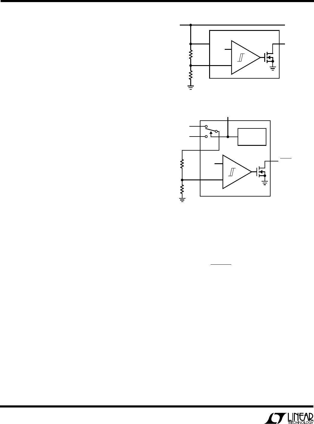
V
GG
Regulator Inductor and Capacitors
The V
GG
regulator provides a power supply voltage signifi-
cantly higher than any of the three main power source
voltages to allow the control of N-channel MOSFET
switches. This 36.5V micropower, step-up voltage regula-
tor is powered by the highest potential available from the
three main power sources for maximum regulator effi-
ciency.
Because the three input supply diodes and regulator
output diode are built into the LTC1479, only three external
components are required by the V
GG
regulator: L1, C1 and
C2 as shown in Figure 7.
L1 is a small, low current 1mH surface mount inductor. C1
provides filtering at the top of the 1mH switched inductor
and should be 1µF to filter switching transients. The V
GG
output capacitor, C2, provides storage and filtering for the
V
GG
output and should be 1µF and rated for 50V operation.
C1 and C2 can be either tantalum or ceramic capacitors.
V
CC
and V
CCP
Regulator Capacitors
The V
CCP
logic supply is approximately 5V and provides
power for the majority of the internal logic circuitry.
Bypass this output with a 0.1µF capacitor.
The V
CC
supply is approximately 3.60V and provides
power for the V
GG
switching regulator control circuitry and
the gate drivers. Bypass this output with a 2.2µF tantalum
capacitor.
This capacitor is required for stability of the V
CC
regulator output
.
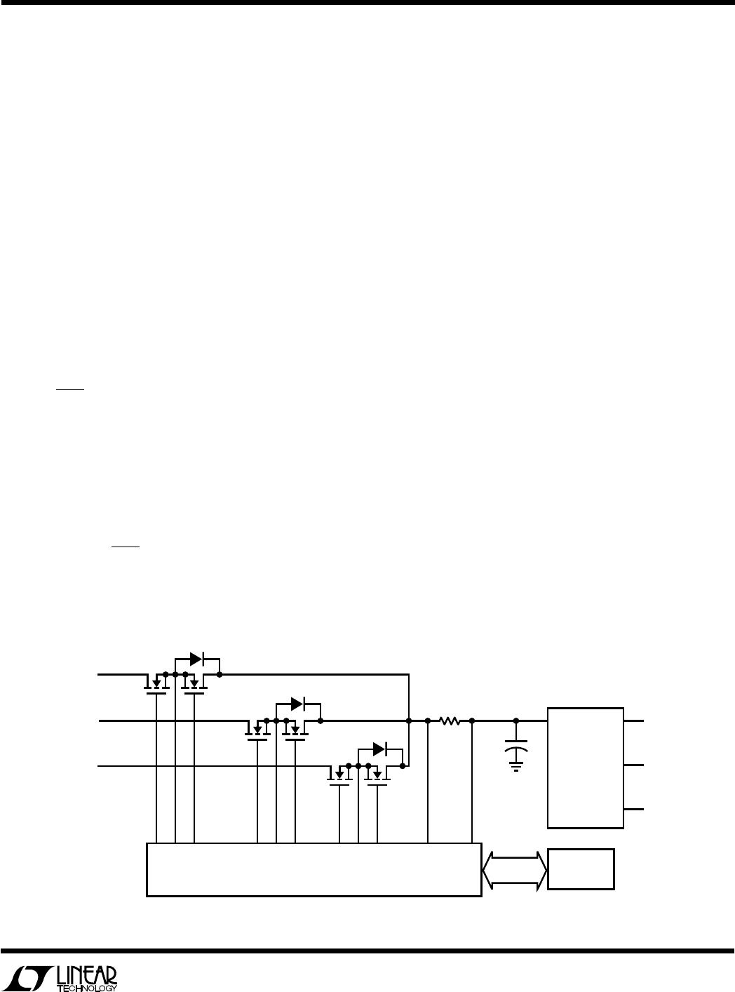
SYSTEM LEVEL CONSIDERATIONS
The Complete Power Management System
The LTC1479 is the “heart” of a complete power manage-
ment system and is responsible for the main power path
and charger switching. A companion power management
µP provides overall control of the power management
system in concert with the LTC1479 and the auxiliary
power management systems.
A typical dual Li-Ion battery power management system is
illustrated in Figure 8. If “good” power is available at the
DCIN input (from the AC adapter), switch pair SW A/B are
turned on—providing a low-loss path for current flow to
the input of the LTC1538-AUX DC/DC converter. Switch
pairs, SW C/D and SW E/F are turned off to block current
from flowing back into the two battery packs from the DC
input.
In this case, an LT1510 constant-voltage/constant-cur-
rent (CC/CV) battery charger circuit is used to alternately
charge the two Li-Ion battery packs. The µP “decides”
which battery is in need of recharging by either querying
the “smart” battery directly or by more indirect means.
After the determination is made, either switch pair, SW G
or SW H, is turned on to pass charger output current to one
of the batteries. Simultaneously, the selected battery volt-
age is returned to the voltage feedback input of the LT1510
CV/CC battery charger via the CHGMON output of the
LTC1479. After the first battery has been charged, it is
disconnected from the charger circuit and the second
battery is connected through the other switch pair and the
second battery charged.
Backup power is provided by the LT1304 circuit which
ensures that the DC/DC input voltage does not drop
below 6V.
Backup System Interface
The LTC1479 is designed to work in concert with related
power management products including the LT1304 mi-
Figure 7. V
GG
Step-Up Switch Regulator
BAT1
BAT2
DCIN
V
+
SW
GND
*COILCRAFT 1812LS-105 XKBC (708) 639-6400
OR EQUIVALENT
1479 F07
V
GG
+
+
L1*
1mH
C1
1µF
35V
C2
1µF
50V
TO GATE
DRIVERS
(36.5V)
LTC1479
V
GG
SWITCHING
REGULATOR