DS1557 4Meg, Nonvolatile, Y2K-Compliant Timekeeping RAM
10 of 17
ABSOLUTE MAXIMUM RATINGS
Voltage Range on Any Pin Relative to Ground………………………………………………………………-0.3V to +6.0V
Storage Temperature Range…………...………………………………………………………….....……..-55°C to +125°C
Lead Temperature (soldering, 10s).....................................................................................................…………+260°C
Soldering Temperature (reflow)………………………………………………………………………………………. +260°C
This is a stress rating only and functional operation of the device at these or any other conditions above those indicated in the operation sections of this
specification is not implied. Exposure to absolute maximum rating conditions for extended periods of time may affect reliability.
OPERATING RANGE
RANGE TEMP RANGE V
CC
Commercial 0°C to +70°C
3.3V 10% or 5V 10%
Industrial -40°C to +85°C
3.3V 10% or 5V 10%
RECOMMENDED DC OPERATING CONDITIONS
(T
A
= Over the Operating Range)
PARAMETER SYMBOL
CONDITIONS
MIN TYP MAX UNITS
V
IH
V
CC
= 5V 10%
2.2
V
CC
+
0.3V
V
Logic 1 Voltage All Inputs
(Note 1)
V
IH
V
CC
= 3.3V 10%
2.0
V
CC
+
0.3V
V
V
IL
V
CC
= 5V 10%
-0.3 +0.8
Logic 0 Voltage All Inputs
(Note 1)
V
IL
V
CC
= 3.3V 10%
-0.3 +0.6
DC ELECTRICAL CHARACTERISTICS
(V
CC
= 5.0V ±10%, T
A
= Over the Operating Range.)
PARAMETER SYMBOL CONDITIONS MIN TYP MAX UNITS
Active Supply Current I
CC
(Notes 2, 3, 11) 45 90 mA
TTL Standby Current
(CE = V
IH
)
I
CC1
(Notes 2, 3) 3 6 mA
CMOS Standby Current
(CE V
CC
- 0.2V)
I
CC2
(Notes 2, 3) 2 6 mA
Input Leakage Current
(Any Input)
I
IL
-1 +1
A
Output Leakage Current
(Any Output)
I
OL
-1 +1
A
Output Logic 1 Voltage
(I
OUT
= -1.0 mA)
V
OH
(Note 1) 2.4 V
V
OL1
I
OUT
= 2.1 mA,
DQ0–7 Outputs
(Note 1)
0.4 V
Output Logic 0 Voltage
V
OL2
I
OUT
= 7.0 mA,
IRQ/FT, and RST
Outputs
(Notes 1, 5)
0.4 V
Write Protection Voltage V
PF
(Note 1) 4.20 4.50 V
Battery Switchover Voltage V
SO
(Notes 1, 4) V
BAT
V
DS1557 4Meg, Nonvolatile, Y2K-Compliant Timekeeping RAM
11 of 17
DC ELECTRICAL CHARACTERISTICS
(V
CC
= 3.3V ±10%, T
A
= Over the Operating Range.)
PARAMETER SYMBOL CONDITIONS MIN TYP MAX UNITS
Active Supply Current I
CC
(Notes 2, 3, 11) 20 30 mA
TTL Standby Current
(CE = V
IH
)
I
CC1
(Notes 2, 3) 2 6 mA
CMOS Standby Current
(CE V
CC
- 0.2V)
I
CC2
(Notes 2, 3) 1 4 mA
Input Leakage Current
(Any Input)
I
IL
-1 +1
A
Output Leakage Current
(Any Output)
I
OL
-1 +1
A
Output Logic 1 Voltage
(I
OUT
= -1.0 mA)
V
OH
(Note 1) 2.4 V
V
OL1
I
OUT
= 2.1 mA, DQ0–7
Outputs (Note 1)
0.4 V
Output Logic 0 Voltage
V
OL2
I
OUT
= 7.0 mA, IRQ/FT
and RST Outputs
(Notes 1, 5)
0.4 V
Write Protection Voltage V
PF
(Note 1) 2.75 2.97 V
Battery Switchover Voltage V
SO
(Notes 1, 4)
V
BAT
or
V
PF
V
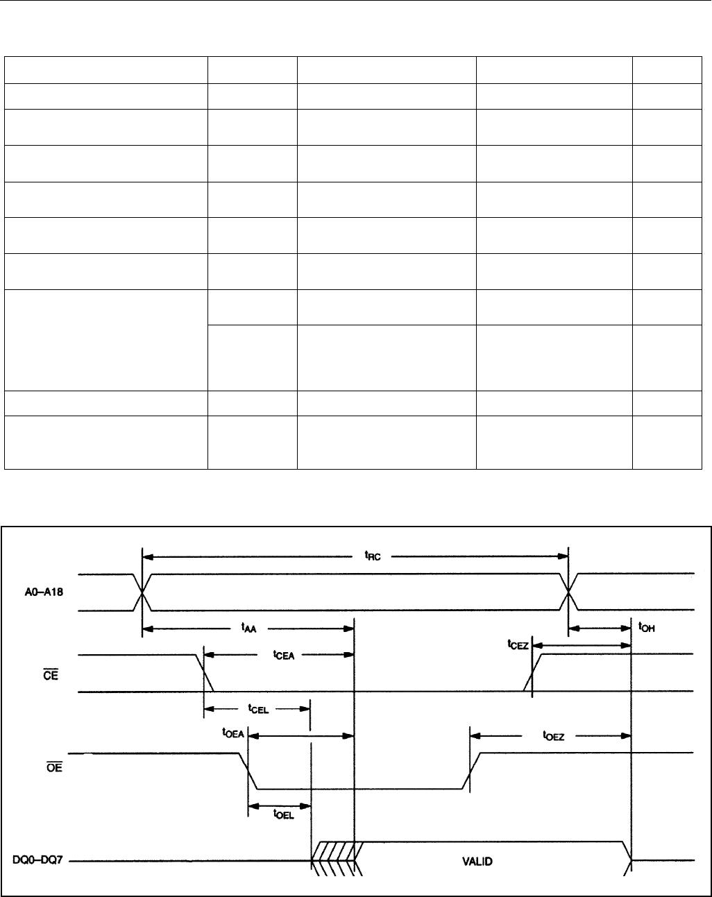
Figure 5. Read Cycle Timing Diagram
DS1557 4Meg, Nonvolatile, Y2K-Compliant Timekeeping RAM
12 of 17
AC CHARACTERISTICS—READ CYCLE
(T
A
= Over the Operating Range)
V
CC
= 5.0V 10% V
CC
= 3.3V 10%
PARAMETER SYMBOL
MIN MAX MIN MAX
UNITS
Read Cycle Time t
RC
70 120 ns
Address Access Time t
AA
70 120 ns
CE to DQ Low-Z
t
CEL
5 5 ns
CE Access Time
t
CEA
70 120 ns
CE Data Off Time
t
CEZ
25 40 ns
OE to DQ Low-Z
t
OEL
5 5 ns
OE Access Time
t
OEA
35 100 ns
OE Data Off Time
t
OEZ
25 35 ns
Output Hold from Address t
OH
5 5 ns
AC CHARACTERISTICS—WRITE CYCLE
(T
A
= Over the Operating Range)
V
CC
= 5.0V 10% V
CC
= 3.3V 10%
PARAMETER SYMBOL
MIN MAX MIN MAX
UNITS
Write Cycle Time t
WC
70 120 ns
Address Access Time t
AS
0 0 ns
WE Pulse Width
t
WEW
50 100 ns
CE Pulse Width
t
CEW
60 110 ns
Data Setup Time t
DS
30 80 ns
Data Hold Time (Note 9) t
DH1
5 5 ns
Data Hold Time (Note 10) t
DH2
5 5 ns
Address Hold Time (Note 9) t
AH1
5 0 ns
Address Hold Time
(Note 10)
t
AH2
5 5 ns
WE Data Off Time
t
WEZ
25 40 ns
Write Recovery Time t
WR
5 10 ns

DS1557WP-120IND+

Mfr. #:
Manufacturer:
Maxim Integrated
Description:
Real Time Clock 4M NV RAM Timekeeper
Lifecycle:
New from this manufacturer.
Delivery:
DHL FedEx Ups TNT EMS
Payment:
T/T Paypal Visa MoneyGram Western Union

Products related to this Datasheet