2
For more information www.linear.com/LTC4355
absolute MaxiMuM ratings
Supply Voltages
IN1, IN2 .................................................. –1V to 100V
OUT ..................................................... –0.3V to 100V
Input Voltages
MON1, MON2, SET .................................. –0.3V to 7V
Output Voltages
GATE1 (Note 3) ................... V
IN1
– 0.2V to V
IN1
+ 13V
GATE2 (Note 3)
................... V
IN2
– 0.2V to V
IN2
+ 13V
PWRFLT1, PWRFLT2, VDSFLT,
FUSEFLT1, FUSEFLT2 ............................... –0.3V to 8V
(Notes 1, 2)
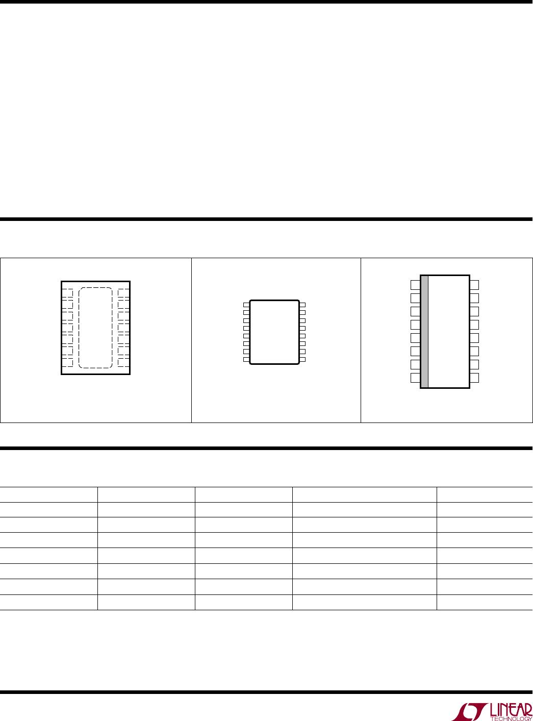
1
2
3
4
5
6
7
14
13
12
11
10
9
8
15
MON1
PWRFLT1
FUSEFLT1
FUSEFLT2
PWRFLT2
MON2
SET
IN1
GATE1
OUT
GATE2
IN2
VDSFLT
GND
DE14 PACKAGE
14-LEAD (4mm × 3mm) PLASTIC DFN
T
JMAX
= 125°C, θ
JA
= 43°C/W
EXPOSED PAD (PIN 15) PCB GND CONNECTION OPTIONAL
1
2
3
4
5
6
7
8
IN1
GATE1
NC
OUT
NC
GATE2
IN2
VDSFLT
16
15
14
13
12
11
10
9
MON1
PWRFLT1
FUSEFLT1
FUSEFLT2
PWRFLT2
MON2
SET
GND
MS PACKAGE
T
JMAX
= 125°C, θ
JA
= 120°C/W
MON1
PWRFLT1
FUSEFLT1
FUSEFLT2
PWRFLT2
MON2
SET
GND
S PACKAGE
1
2
3
4
5
6
7
8
16
15
14
13
12
11
10
9
IN1
GATE1
NC
OUT
NC
GATE2
IN2
NC
T
JMAX
= 125°C, θ
JA
= 80°C/W
Operating Ambient Temperature Range
LTC4355C ................................................ 0°C to 70°C
LTC4355I..............................................–40°C to 85°C
LTC4355H ..........................................–40°C to 125°C
Storage Temperature Range ...................–65°C to 150°C
Lead Temperature (Soldering, 10 sec)
MS, SO Packages ............................................. 300°C
LEAD FREE FINISH TAPE AND REEL PART MARKING* PACKAGE DESCRIPTION TEMPERATURE RANGE
LTC4355CDE#PBF LTC4355CDE#TRPBF 4355
14-Lead (4mm × 3mm) Plastic DFN
0°C to 70°C
LTC4355IDE#PBF LTC4355IDE#TRPBF 4355
14-Lead (4mm × 3mm) Plastic DFN
–40°C to 85°C
LTC4355CS#PBF LTC4355CS#TRPBF LTC4355CS 16-Lead Plastic SO 0°C to 70°C
LTC4355IS#PBF LTC4355IS#TRPBF LTC4355IS 16-Lead Plastic SO –40°C to 85°C
LTC4355CMS#PBF LTC4355CMS#TRPBF 4355 16-Lead Plastic MSOP 0°C to 70°C
LTC4355IMS#PBF LTC4355IMS#TRPBF 4355 16-Lead Plastic MSOP –40°C to 85°C
LTC4355HMS#PBF LTC4355HMS#TRPBF 4355 16-Lead Plastic MSOP –40°C to 125°C
Consult LTC Marketing for parts specified with wider operating temperature ranges. *Temperature grades are identified by a label on the shipping container.
Consult LTC Marketing for information on non-standard lead based finish parts.
For more information on lead free part marking, go to: http://www.linear.com/leadfree/
For more information on tape and reel specifications, go to: http://www.linear.com/tapeandreel/
pin conFiguration
orDer inForMation