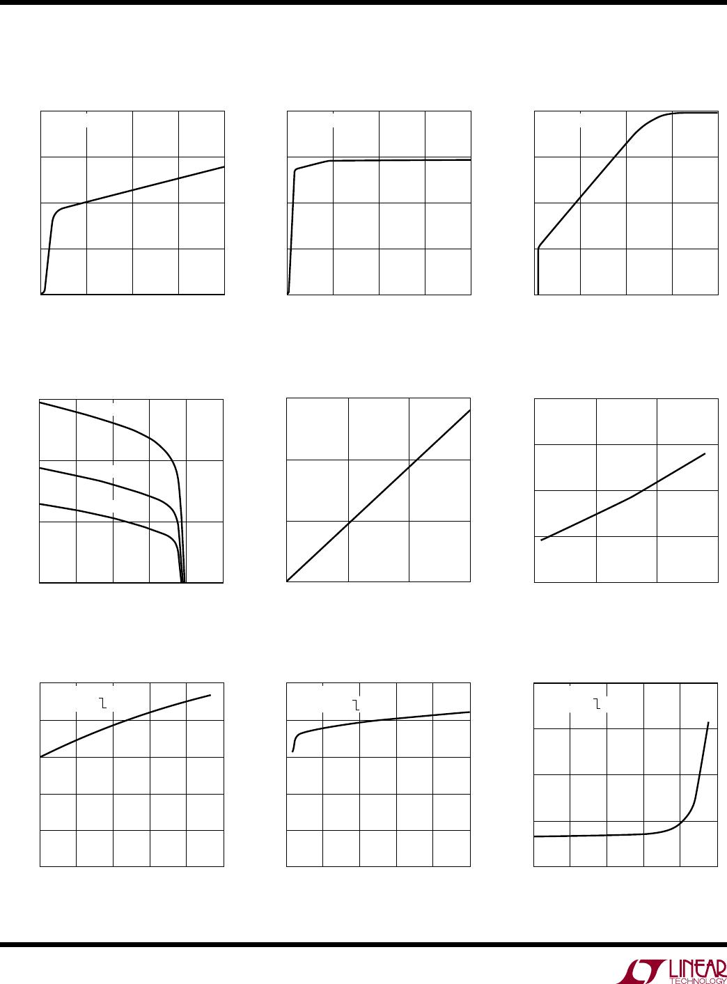
5
For more information www.linear.com/LTC4355
pin Functions
Exposed Pad: Exposed pad may be left open or connected
to GND.
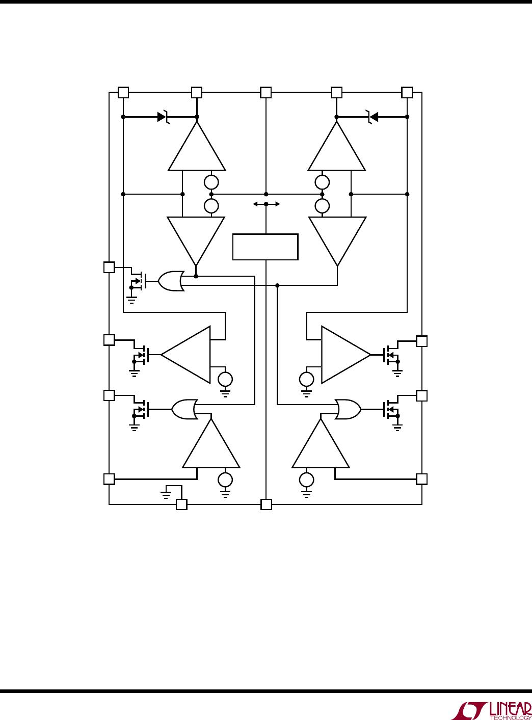
FUSEFLTx: Fuse Fault Outputs. Open-drain output that
pulls to GND when V
INx
< 3.5V, indicating that the fuse
has blown open. Otherwise, this output is high impedance.
Connect to GND if unused.
GATEx: Gate Drive Outputs. The GATE pins pull high,
enhancing the N-channel MOSFET when the load cur
-
rent creates more than 25mV of voltage drop across
t
he MOSFE
T. When the load current is small, the
gates are actively driven to maintain 25mV across the
MOSFET. If the reverse current develops more than
–25mV of voltage drop across a MOSFET, a fast pull-down
circu
it quickly connects the GATE pin to the IN pin, turning
off the MOSFET. Limit the capacitance between the GATE
and IN pins to less than 0.1µF.
GND: Device Ground.
INx: Input Voltages and GATE Fast Pull-Down Returns. The
IN pins are the anodes of the ideal diodes and connect to the
sources of the N-channel MOSFETs. The voltages sensed
at these pins are used to control the source-drain voltages
across the MOSFETs and are used by the fault detection
circuits that drive the PWR FLT, FUSEFLT, and VD SFLT pins.
The GATE fast pull-down current is returned through the IN
pins. Connect these pins as close to the MOSFET sources
as possible. Connect to OUT if unused.
MONx: Input Supply Monitors. These pins are used to
sense the input supply voltages. Connect these pins to
external resistive dividers between the input supplies and
GND. If V
MONx
falls below 1.23V, the PWRFLTx pin pulls
to GND. Connect to GND if unused.
NC: No Connection. Not internally connected. These
pins provide extra distance between high and low volt-
age pins.
O
UT: Drain Voltage Sense and Positive Supply Input. OUT
is the diode-OR output of IN1 and IN2. It connects to the
common drain connection of the N-channel MOSFETs. The
voltage sensed at this pin is used to control the source-
drain voltages across the MOSFETs and is used by the
fault detection circuits that drive the PWRFLT and VD SFLT
pins. The LTC4355 is powered from the OUT pin.
PWR FLTx: Power Fault Outputs. Open-drain output
that pulls to GND when V
MONx
falls below 1.23V or
the forward voltage across the MOSFET exceeds
DV
SD(FLT)
. When V
MONx
is above 1.23V and the
forward voltage across the MOSFET is less than
DV
SD(FLT)
, PWRFLTx is high impedance. Connect to GND
if unused.
SET: DV
SD(FLT)
Threshold Configuration Input. Tying SET
to GND, to a 100k resistor connected to GND, or leaving
SET open configures the DV
SD(FLT)
forward voltage fault
threshold to 250mV, 500mV, or 1.5V, respectively. When the
voltage across a MOSFET exceeds DV
SD(FLT)
, the VSD FLT
pin and at least one of the PWR FLT pins pull to GND.
VDSFLT: MOSFET Fault Output. Open-drain output that
pulls to GND when the forward voltage across either
MOSFET exceeds DV
SD(FLT)
. PWRFLT1 or PWR FLT2 also
pulls low to indicate which MOSFET’s forward voltage drop
exceeds DV
SD(FLT)
. Otherwise, this pin is high impedance.
Connect to GND if unused.