LTC2607/LTC2617/LTC2627
1
26071727fa
Block Diagram
Features Description
16-/14-/12-Bit Dual Rail-to-Rail
DACs with I
2
C Interface
The LTC
®
2607/LTC2617/LTC2627 are dual 16-, 14- and
12-bit, 2.7V to 5.5V rail-to-rail voltage output DACs in a
12-lead DFN package. They have built-in high performance
output buffers and are guaranteed monotonic.
These parts establish new board-density benchmarks for
16- and 14-bit DACs and advance performance standards
for output drive and load regulation in single-supply,
voltage-output DACs.
The parts use a 2-wire, I
2
C compatible serial interface. The
LTC2607/LTC2617/LTC2627 operate in both the standard
mode (clock rate of 100kHz) and the fast mode (clock rate
of 400kHz). An asynchronous DAC update pin (LDAC) is
also included.
The LTC2607/LTC2617/LTC2627 incorporate a power-on
reset circuit. During power-up, the voltage outputs rise less
than 10mV above zero scale; and after power-up, they stay
at zero scale until a valid write and update take place. The
power-on reset circuit resets the LTC2607-1/LTC2617-1/
LTC2627-1 to mid-scale. The voltage outputs stay at mid-
scale until a valid write and update takes place.
L, LT, LTC, LTM, Linear Technology and the Linear logo are registered trademarks of Linear
Technology Corporation. All other trademarks are the property of their respective owners.
Protected by U.S. Patents including 5396245 and 6891433. Patent Pending.
applications
n
Smallest Pin-Compatible Dual DACs:
LTC2607: 16 Bits
LTC2617: 14 Bits
LTC2627: 12 Bits
n
Guaranteed Monotonic Over Temperature
n
27 Selectable Addresses
n
400kHz I
2
C Interface
n
Wide 2.7V to 5.5V Supply Range
n
Low Power Operation: 260µA per DAC at 3V
n
Power Down to 1µA, Max
n
High Rail-to-Rail Output Drive (±15mA, Min)
n
Ultralow Crosstalk (30µV)
n
Double-Buffered Data Latches
n
Asynchronous DAC Update Pin
n
LTC2607/LTC2617/LTC2627: Power-On Reset to
Zero Scale
n
LTC2607-1/LTC2617-1/LTC2627-1: Power-On Reset
to Mid-Scale
n
Tiny (3mm × 4mm) 12-Lead DFN Package
n
Mobile Communications
n
Process Control and Industrial Automation
n
Instrumentation
n
Automatic Test Equipment
Differential Nonlinearity
(LTC2607)
9
811 10
5 6
21 43
2-WIRE INTERFACE
CA0 CA1 LDAC SCL SDA
REFLO GND REF V
CC
CA2
32-BIT SHIFT REGISTER
INPUT REGISTER INPUT REGISTER
DAC REGISTER DAC REGISTER
7
12-/14-/16-BIT DAC
V
OUTB
12
12-/14-/16-BIT DAC
V
OUTA
2607 BD01a
CODE
0 16384 32768 49152 65535
DNL (LSB)
2607 BD01b
1.0
0.8
0.6
0.4
0.2
0
–0.2
–0.4
–0.6
–0.8
–1.0
V
CC
= 5V
V
REF
= 4.096V
LTC2607/LTC2617/LTC2627
2
26071727fa
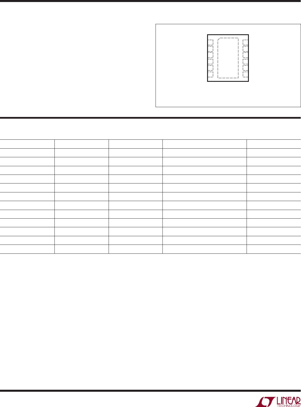
pin conFigurationaBsolute maximum ratings
Any Pin to GND ............................................ 0.3V to 6V
Any Pin to V
CC
............................................. 6V to 0.3V
Maximum Junction Temperature .......................... 125°C
Storage Temperature Range .................. 65°C to 125°C
Lead Temperature (Soldering, 10 sec)...................300°C
Operating Temperature Range:
LTC2607C/LTC2617C/LTC2627C
LTC2607C-1/LTC2617C-1/LTC2627C-1 .... 0°C to 70°C
LTC2607I/LTC2617I/LTC2627I
LTC2607I-1/LTC2617I-1/LTC2627I-1 ....40°C to 85°C
(Note 1)
TOP VIEW
13
DE12 PACKAGE
12-LEAD (4mm s 3mm) PLASTIC DFN
12
11
8
9
10
4
5
3
2
1
V
OUTA
REFLO
GND
REF
V
CC
V
OUTB
CA0
CA1
LDAC
SCL
SDA
CA2
7
6
T
JMAX
= 125°C, θ
JA
= 43°C/W
EXPOSED PAD (PIN 13) IS GND, MUST BE SOLDERED TO PCB
orDer inFormation
LEAD FREE FINISH TAPE AND REEL PART MARKING* PACKAGE DESCRIPTION TEMPERATURE RANGE
LTC2607CDE#PBF LTC2607CDE#TRPBF 2607
12-Lead (4mm × 3mm) Plastic DFN
0°C to 70°C
LTC2607IDE#PBF LTC2607IDE#TRPBF 2607
12-Lead (4mm × 3mm) Plastic DFN
–40°C to 85°C
LTC2607CDE-1#PBF LTC2607CDE-1#TRPBF 26071
12-Lead (4mm × 3mm) Plastic DFN
0°C to 70°C
LTC2607IDE-1#PBF LTC2607IDE-1#TRPBF 26071
12-Lead (4mm × 3mm) Plastic DFN
–40°C to 85°C
LTC2617CDE#PBF LTC2617CDE#TRPBF 2617
12-Lead (4mm × 3mm) Plastic DFN
0°C to 70°C
LTC2617IDE#PBF LTC2617IDE#TRPBF 2617
12-Lead (4mm × 3mm) Plastic DFN
–40°C to 85°C
LTC2617CDE-1#PBF LTC2617CDE-1#TRPBF 26171
12-Lead (4mm × 3mm) Plastic DFN
0°C to 70°C
LTC2617IDE-1#PBF LTC2617IDE-1#TRPBF 26171
12-Lead (4mm × 3mm) Plastic DFN
–40°C to 85°C
LTC2627CDE#PBF LTC2627CDE#TRPBF 2627
12-Lead (4mm × 3mm) Plastic DFN
0°C to 70°C
LTC2627IDE#PBF LTC2627IDE#TRPBF 2627
12-Lead (4mm × 3mm) Plastic DFN
–40°C to 85°C
LTC2627CDE-1#PBF LTC2627CDE-1#TRPBF 26271
12-Lead (4mm × 3mm) Plastic DFN
0°C to 70°C
LTC2627IDE-1#PBF LTC2627IDE-1#TRPBF 26271
12-Lead (4mm × 3mm) Plastic DFN
–40°C to 85°C
Consult LTC Marketing for parts specified with wider operating temperature ranges. *The temperature grade is identified by a label on the shipping container.
Consult LTC Marketing for information on non-standard lead based finish parts.
For more information on lead free part marking, go to: http://www.linear.com/leadfree/
For more information on tape and reel specifications, go to: http://www.linear.com/tapeandreel/
LTC2607/LTC2617/LTC2627
3
26071727fa
electrical characteristics
The l denotes the specifications which apply over the full operating
temperature range, otherwise specifications are at T
A
= 25°C. REF = 4.096V (V
CC
= 5V), REF = 2.048V (V
CC
= 2.7V), REFLO = 0V,
V
OUT
unloaded, unless otherwise noted.
SYMBOL PARAMETER CONDITIONS
LTC2627/LTC2627-1 LTC2617/LTC2617-1 LTC2607/LTC2607-1
UNITSMIN TYP MAX MIN TYP MAX MIN TYP MAX
DC Performance
Resolution
l
12 14 16 Bits
Monotonicity (Note 2)
l
12 14 16 Bits
DNL Differential Nonlinearity (Note 2)
l
±0.5 ±1 ±1 LSB
INL Integral Nonlinearity (Note 2)
l
±1.5 ±4 ±5 ±16 ±19 ±64 LSB
Load Regulation V
REF
= V
CC
= 5V, Mid-Scale
I
OUT
= 0mA to 15mA Sourcing
I
OUT
= 0mA to 15mA Sinking
l
l
0.02
0.03
0.125
0.125
0.1
0.1
0.5
0.5
0.35
0.42
2
2
LSB/mA
LSB/mA
V
REF
= V
CC
= 2.7V, Mid-Scale
I
OUT
= 0mA to 7.5mA Sourcing
I
OUT
= 0mA to 7.5mA Sinking
l
l
0.04
0.05
0.25
0.25
0.2
0.2
1
1
0.7
0.8
4
4
LSB/mA
LSB/mA
ZSE Zero-Scale Error Code = 0
l
1 9 1 9 1 9 mV
V
OS
Offset Error (Note 6)
l
±1 ±9 ±1 ±9 ±1 ±9 mV
V
OS
Temperature
Coefficient
±7 ±7 ±7 µV/°C
GE Gain Error
l
±0.15 ±0.7 ±0.15 ±0.7 ±0.15 ±0.7 %FSR
Gain Temperature
Coefficient
±4 ±4 ±4 ppm/°C
The l denotes the specifications which apply over the full operating temperature range, otherwise specifications are at T
A
= 25°C.
REF = 4.096V (V
CC
= 5V), REF = 2.048V (V
CC
= 2.7V), REFLO = 0V, V
OUT
unloaded, unless otherwise noted.
SYMBOL PARAMETER CONDITIONS MIN TYP MAX UNITS
PSR Power Supply Rejection V
CC
±10% –80 dB
R
OUT
DC Output Impedance V
REF
= V
CC
= 5V, Mid-Scale;
–15mA ≤ I
OUT
≤ 15mA
V
REF
= V
CC
= 2.7V, Mid-Scale;
–7.5mA ≤ I
OUT
≤ 7.5mA
l
l
0.032
0.035
0.15
0.15
Ω
Ω
DC Crosstalk (Note 4) Due to Full Scale Output Change (Note 5)
Due to Load Current Change
Due to Powering Down (Per Channel)
±4
±3
±30
µV
µV/mA
µV
I
SC
Short-Circuit Output Current V
CC
= 5.5V, V
REF
= 5.5V
Code: Zero Scale; Forcing Output to V
CC
Code: Full Scale; Forcing Output to GND
l
l
15
15
36
37
60
60
mA
mA
V
CC
= 2.7V, V
REF
= 2.7V
Code: Zero Scale; Forcing Output to V
CC
Code: Full Scale; Forcing Output to GND
l
l
7.5
7.5
22
30
50
50
mA
mA
Reference Input
Input Voltage Range
l
0 V
CC
V
Resistance Normal Mode
l
44 64 80
Capacitance 30 pF
I
REF
Reference Current, Power Down Mode DAC Powered Down
l
0.001 1 µA

LTC2607IDE#PBF

Mfr. #:
Manufacturer:
Analog Devices Inc.
Description:
Digital to Analog Converters - DAC 16-B 2x R2R DACs w/ I2C Int
Lifecycle:
New from this manufacturer.
Delivery:
DHL FedEx Ups TNT EMS
Payment:
T/T Paypal Visa MoneyGram Western Union