LTC2607/LTC2617/LTC2627
13
26071727fa
operation
specifications. For an I
2
C bus operating in the fast mode,
an active pull-up will be necessary if the bus capacitance is
greater than 200pF. The V
CC
power should not be removed
from the LTC2607/LTC2617/LTC2627 when the I
2
C bus
is active to avoid loading the I
2
C bus lines through the
internal ESD protection diodes.
The LTC2607/LTC2617/LTC2627 are receive-only (slave)
devices. The master can write to the LTC2607/LTC2617/
LTC2627. The LTC2607/LTC2617/LTC2627 do not respond
to a read from the master.
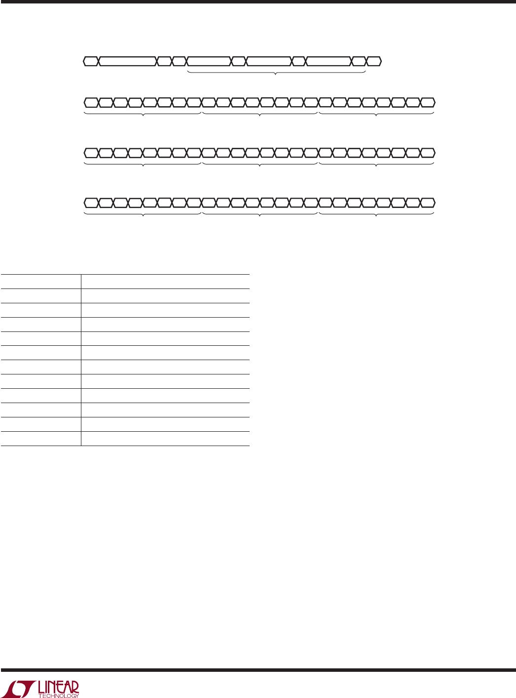
The START (S) and STOP (P) Conditions
When the bus is not in use, both SCL and SDA must be
high. A bus master signals the beginning of a communica-
tion to a slave device by transmitting a START condition. A
START condition is generated by transitioning SDA from
high to low while SCL is high.
When the master has finished communicating with the
slave, it issues a STOP condition. A STOP condition is
generated by transitioning SDA from low to high while
SCL is high. The bus is then free for communication with
another I
2
C device.
Acknowledge
The Acknowledge signal is used for handshaking between
the master and the slave. An Acknowledge (active LOW)
generated by the slave lets the master know that the lat-
est byte of information was received. The Acknowledge
related clock pulse is generated by the master. The master
releases the SDA line (HIGH) during the Acknowledge clock
pulse. The slave-receiver must pull down the SDA bus line
during the Acknowledge clock pulse so that it remains a
stable LOW during the HIGH period of this clock pulse.
The LTC2607/LTC2617/LTC2627 respond to a write by a
master in this manner. The LTC2607/LTC2617/LTC2627
do not acknowledge a read (retains SDA HIGH during the
period of the Acknowledge clock pulse).
Chip Address
The state of CA0, CA1 and CA2 decides the slave address
of the part. The pins CA0, CA1 and CA2 can be each set
to any one of three states: V
CC
, GND or float. This results
Power-On Reset
The LTC2607/LTC2617/LTC2627 clear the outputs to
zero scale when power is first applied, making system
initialization consistent and repeatable. The LTC2607-1/
L
TC2617-
1/LTC2627-1 set the voltage outputs to midscale
when power is first applied.
For some applications, downstream circuits are active
during DAC power-up, and may be sensitive to nonzero
outputs from the DAC during this time. The LTC2607/
LTC2617/LTC2627 contain circuitry to reduce the power-
on glitch; furthermore, the glitch amplitude can be made
arbitrarily small by reducing the ramp rate of the power
supply. For example, if the power supply is ramped to 5V
in 1ms, the analog outputs rise less than 10mV above
ground (typ) during power-on. See Power-On Reset Glitch
in the Typical Performance Characteristics section.
Power Supply Sequencing
The voltage at REF (Pin 9) should be kept within the range
–0.3V ≤ V
REF
≤ V
CC
+ 0.3V (see Absolute Maximum Rat-
ings). Particular care should be taken to observe these
limits during power supply turn-on and turn-off sequences,
when the voltage at V
CC
(Pin 8) is in transition.
Transfer Function
The digital-to-analog transfer function is:
V
k
V V V
OUT IDEAL
N
REF REFLO REFLO( )
=
( )
+
2
where k is the decimal equivalent of the binary DAC
input code, N is the resolution and V
REF
is the voltage at
REF (Pin 6).
Serial Digital Interface
The LTC2607/LTC2617/LTC2627 communicate with a
host using the standard 2-wire I
2
C interface. The Timing
Diagrams (Figures 1 and 2) show the timing relationship
of the signals on the bus. The two bus lines, SDA and
SCL, must be high when the bus is not in use. External
pull-up resistors or current sources are required on these
lines. The value of these pull-up resistors is dependent
on the power supply and can be obtained from the I
2
C
LTC2607/LTC2617/LTC2627
14
26071727fa
in 27 selectable addresses for the part. The slave address
assignments are shown in Table 1.
Table 1. Slave Address Map
CA2 CA1 CA0 SA6 SA5 SA4 SA3 SA2 SA1 SA0
GND GND GND 0 0 1 0 0 0 0
GND GND FLOAT 0 0 1 0 0 0 1
GND GND V
CC
0 0 1 0 0 1 0
GND FLOAT GND 0 0 1 0 0 1 1
GND FLOAT FLOAT 0 1 0 0 0 0 0
GND FLOAT V
CC
0 1 0 0 0 0 1
GND V
CC
GND 0 1 0 0 0 1 0
GND V
CC
FLOAT 0 1 0 0 0 1 1
GND V
CC
V
CC
0 1 1 0 0 0 0
FLOAT GND GND 0 1 1 0 0 0 1
FLOAT GND FLOAT 0 1 1 0 0 1 0
FLOAT GND V
CC
0 1 1 0 0 1 1
FLOAT FLOAT GND 1 0 0 0 0 0 0
FLOAT FLOAT FLOAT 1 0 0 0 0 0 1
FLOAT FLOAT V
CC
1 0 0 0 0 1 0
FLOAT V
CC
GND 1 0 0 0 0 1 1
FLOAT V
CC
FLOAT 1 0 1 0 0 0 0
FLOAT V
CC
V
CC
1 0 1 0 0 0 1
V
CC
GND GND 1 0 1 0 0 1 0
V
CC
GND FLOAT 1 0 1 0 0 1 1
V
CC
GND V
CC
1 1 0 0 0 0 0
V
CC
FLOAT GND 1 1 0 0 0 0 1
V
CC
FLOAT FLOAT 1 1 0 0 0 1 0
V
CC
FLOAT V
CC
1 1 0 0 0 1 1
V
CC
V
CC
GND 1 1 1 0 0 0 0
V
CC
V
CC
FLOAT 1 1 1 0 0 0 1
V
CC
V
CC
V
CC
1 1 1 0 0 1 0
GLOBAL ADDRESS 1 1 1 0 0 1 1
In addition to the address selected by the address pins,
the parts also respond to a global address. This address
allows a common write to all LTC2607, LTC2617 and
LTC2627 parts to be accomplished with one 3-byte write
transaction on the I
2
C bus. The global address is a 7-bit
on-chip hardwired address and is not selectable by CA0,
CA1 and CA2.
operation
The addresses corresponding to the states of CA0, CA1
and CA2 and the global address are shown in Table 1. The
maximum capacitive load allowed on the address pins
(CA0, CA1 and CA2) is 10pF, as these pins are driven during
address detection to determine if they are floating.
Write Word Protocol
The master initiates communication with the LTC2607/
LTC2617/LTC2627 with a START condition and a 7-bit slave
address followed by the Write bit (W) = 0. The LTC2607/
LTC2617/LTC2627 acknowledges by pulling the SDA pin
low at the 9th clock if the 7-bit slave address matches the
address of the parts (set by CA0, CA1 and CA2) or the
global address. The master then transmits three bytes of
data. The LTC2607/LTC2617/LTC2627 acknowledges each
byte of data by pulling the SDA line low at the 9th clock of
each data byte transmission. After receiving three complete
bytes of data, the LTC2607/LTC2617/LTC2627 executes the
command specified in the 24-bit input word.
If more than three data bytes are transmitted after a valid
7-bit slave address, the LTC2607/LTC2617/LTC2627 do not
acknowledge the extra bytes of data (SDA is high during
the 9th clock).
The format of the three data bytes is shown in Figure 3.
The first byte of the input word consists of the 4-bit com-
mand word C3-C0, and 4-bit DAC address A3-A0. The next
two bytes consist of the 16-bit data word. The 16-bit data
word consists of the 16-, 14- or 12-bit input code, MSB
to LSB, followed by 0, 2 or 4 don’t care bits (LTC2607,
LTC2617 and LTC2627 respectively). A typical LTC2607
write transaction is shown in Figure 4.
The command (C3-C0) and address (A3-A0) assignments
are shown in Table 2. The first four commands in the table
consist of write and update operations. A write operation
loads a 16-bit data word from the 32-bit shift register
into the input register of the selected DAC, n. An update
operation copies the data word from the input register to
the DAC register. Once copied into the DAC register, the
data word becomes the active 16-, 14- or 12-bit input
code, and is converted to an analog voltage at the DAC
output. The update operation also powers up the selected
DAC if it had been in power-down mode. The data path
and registers are shown in the Block Diagram.
LTC2607/LTC2617/LTC2627
15
26071727fa
operation
Table 2
COMMAND*
C3 C2 C1 C0
0 0 0 0 Write to Input Register
0 0 0 1 Update (Power Up) DAC Register
0 0 1 1 Write to and Update (Power Up)
0 1 0 0 Power Down
1 1 1 1 No Operation
ADDRESS*
A3 A2 A1 A0
0 0 0 0 DAC A
0 0 0 1 DAC B
1 1 1 1 All DACs
*Command and address codes not shown are reserved and should not be used.
Power-Down Mode
For power-constrained applications, the power-down mode
can be used to reduce the supply current whenever one or
both of the DAC outputs are not needed. When in power-
down, the buffer amplifiers, bias circuits and reference input
are disabled and draw essentially zero current. The DAC
outputs are put into a high impedance state, and the output
pins are passively pulled to V
REFLO
through 90k resistors.
Input-register and DAC-register contents are not disturbed
during power-down.
Either or both DAC channels can be put into power-down
mode by using command 0100b in combination with the
Figure 3
C3
1ST DATA BYTE
Input Word (LTC2607)
Write Word Protocol for LTC2607/LTC2617/LTC1627
C2
C1
C0
A3
A2
A1
A0
D13D14D15
S
W A
SLAVE ADDRESS
1ST DATA BYTE
D12
D11 D10 D9 D8
D7
D6
D5 D4 D3 D2 D1
D0
A 2ND DATA BYTE A 3RD DATA BYTE A P
2607 F03
2ND DATA BYTE
INPUT WORD
3RD DATA BYTE
C3
1ST DATA BYTE
Input Word (LTC2617)
C2
C1
C0
A3
A2
A1
A0
D11D12D13
D10
D9 D8 D7 D6
D5
D4
D3 D2 D1 D0 X
X
2ND DATA BYTE 3RD DATA BYTE
C3
1ST DATA BYTE
Input Word (LTC2627)
C2
C1
C0
A3
A2
A1
A0
D9D10D11
D8
D7 D6 D5 D4
D3
D2
D1 D0 X X X
X
2ND DATA BYTE 3RD DATA BYTE
appropriate DAC address. The 16-bit data word is ignored.
The supply and reference currents are reduced by approxi-
mately 50% for each DAC powered down; the effective
resistance at REF (Pin 9) rises accordingly, becoming a
high-impedance input (typically > 1GΩ) when both DACs
are powered down.
Normal operation can be resumed by executing any
command which includes a DAC update, as shown in
Table 2 or performing an asychronous update (LDAC) as
described in the next section. The selected DAC is powered
up as its voltage output is updated. When a DAC in powered-
down state is powered up and updated, normal settling
is delayed. If one of the two DACs is in a powered- down
state prior to the update command, the power up delay is
5µs. If on the other hand, both DACs are powered down,
the main bias generation circuit has been automatically
shut down in addition to the DAC amplifiers and reference
input and so the power up delay time is
12µs (for V
CC
= 5V) or 30µs (for V
CC
= 3V)
Asynchronous DAC Update Using LDAC
In addition to the update commands shown in Table 2, the
LDAC pin asynchronously updates the DAC registers with
the contents of the input registers. Asynchronous update
is disabled when the input word is being clocked into
the part.

LTC2607IDE#PBF

Mfr. #:
Manufacturer:
Analog Devices Inc.
Description:
Digital to Analog Converters - DAC 16-B 2x R2R DACs w/ I2C Int
Lifecycle:
New from this manufacturer.
Delivery:
DHL FedEx Ups TNT EMS
Payment:
T/T Paypal Visa MoneyGram Western Union