LTC2607/LTC2617/LTC2627
5
26071727fa
electrical characteristics
timing characteristics
Note 1: Stresses beyond those listed under Absolute Maximum Ratings
may cause permanent damage to the device. Exposure to any Absolute
Maximum Rating condition for extended periods may affect device
reliability and lifetime.
Note 2: Linearity and monotonicity are defined from code k
L
to code
2N – 1, where N is the resolution and k
L
is given by k
L
= 0.016(2
N
/V
REF
),
rounded to the nearest whole code. For V
REF
= 4.096V and N = 16, k
L
=
256 and linearity is defined from code 256 to code 65,535.
Note 3: SDA, SCL and LDAC at 0V or V
CC
, CA0, CA1 and CA2 Floating.
Note 4: DC crosstalk is measured with V
CC
= 5V and V
REF
= 4.096V, with
the measured DAC at mid-scale, unless otherwise noted.
SYMBOL PARAMETER CONDITIONS MIN TYP MAX UNITS
V
CC
= 2.7V to 5.5V
f
SCL
SCL Clock Frequency
l
0 400 kHz
t
HD(STA)
Hold Time (Repeated) Start Condition
l
0.6 µs
t
LOW
Low Period of the SCL Clock Pin
l
1.3 µs
t
HIGH
High Period of the SCL Clock Pin
l
0.6 µs
t
SU(STA)
Set-Up Time for a Repeated Start Condition
l
0.6 µs
t
HD(DAT)
Data Hold Time
l
0 0.9 µs
t
SU(DAT)
Data Set-Up Time
l
100 ns
t
r
Rise Time of Both SDA and SCL Signals (Note 9)
l
20 + 0.1C
B
300 ns
t
f
Fall Time of Both SDA and SCL Signals (Note 9)
l
20 + 0.1C
B
300 ns
t
SU(STO)
Set-Up Time for Stop Condition
l
0.6 µs
t
BUF
Bus Free Time Between a Stop and Start Condition
l
1.3 µs
t
1
Falling Edge of 9th Clock of the 3rd Input Byte to
LDAC High or Low Transition
l
400 ns
t
2
LDAC Low Pulse Width
l
20 ns
The l denotes the specifications which apply over the full operating temperature
range, otherwise specifications are at T
A
= 25°C. (See Figure 1) (Notes 10, 11)
The
l denotes the specifications which apply over the full operating
temperature range, otherwise specifications are at T
A
= 25°C. REF = 4.096V (V
CC
= 5V), REF = 2.048V (V
CC
= 2.7V), REFLO = 0V,
V
OUT
unloaded, unless otherwise noted.
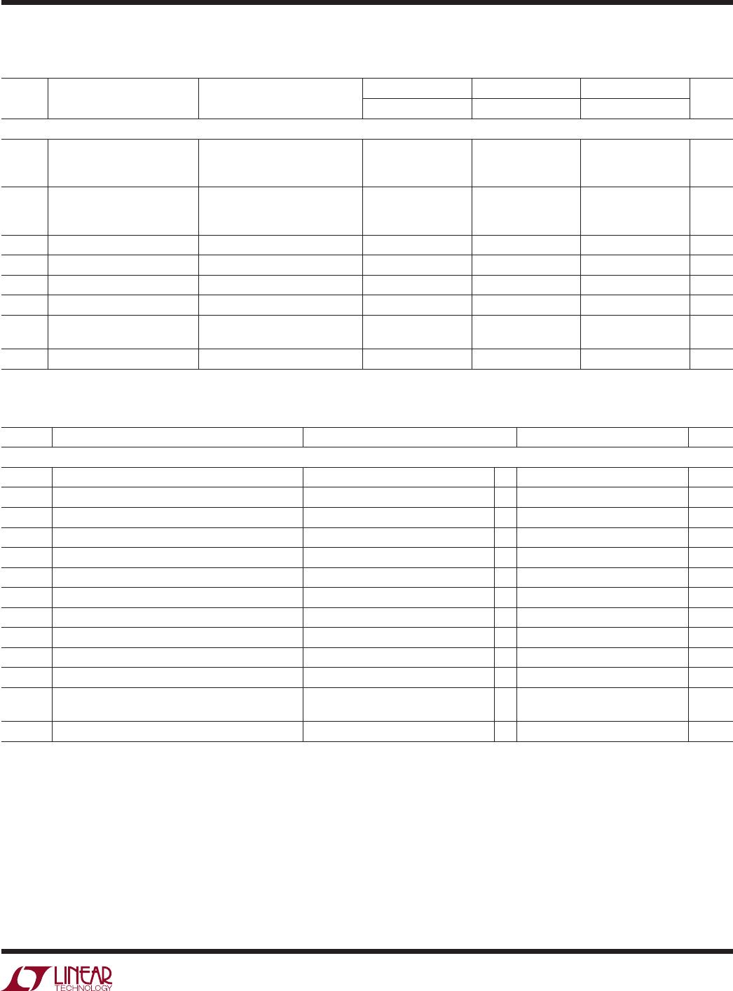
SYMBOL PARAMETER CONDITIONS
LTC2627/LTC2627-1 LTC2617/LTC2617-1 LTC2607/LTC2607-1
UNITSMIN TYP MAX MIN TYP MAX MIN TYP MAX
AC Performance
t
S
Settling Time (Note 7) ±0.024% (±1LSB at 12 Bits)
±0.006% (±1LSB at 14 Bits)
±0.0015% (±1LSB at 16 Bits)
7 7
9
7
9
10
µs
µs
µs
Settling Time for 1LSB Step
(Note 8)
±0.024% (±1LSB at 12 Bits)
±0.006% (±1LSB at 14 Bits)
±0.0015% (±1LSB at 16 Bits)
2.7 2.7
4.8
2.7
4.8
5.2
µs
µs
µs
Voltage Output Slew Rate 0.8 0.8 0.8 V/µs
Capacitive Load Driving 1000 1000 1000 pF
Glitch Impulse At Mid-Scale Transition 12 12 12 nV • s
Multiplying Bandwidth 180 180 180 kHz
e
n
Output Voltage Noise Density At f = 1kHz
At f = 10kHz
120
100
120
100
120
100
nV/√Hz
nV/√Hz
Output Voltage Noise 0.1Hz to 10Hz 15 15 15 µV
P-P
Note 5: R
L
= 2kΩ to GND or V
CC
.
Note 6: Inferred from measurement at code k
L
(Note 2) and at full scale.
Note 7: V
CC
= 5V, V
REF
= 4.096V. DAC is stepped 1/4 scale to 3/4 scale
and 3/4 scale to 1/4 scale. Load is 2k in parallel with 200pF to GND.
Note 8: V
CC
= 5V, V
REF
= 4.096V. DAC is stepped ±1LSB between half
scale and half scale – 1. Load is 2k in parallel with 200pF to GND.
Note 9: C
B
= capacitance of one bus line in pF.
Note 10: All values refer to V
IH(MIN)
and V
IL(MAX)
levels.
Note 11: These specifications apply to LTC2607/LTC2607-1,
LTC2617/LTC2617-1, LTC2627/LTC2627-1.
Note 12: Guaranteed by design and not production tested.