ICS9DB803D
EIGHT OUTPUT DIFFERENTIAL BUFFER FOR PCIE GEN1 AND GEN2
IDT®
EIGHT OUTPUT DIFFERENTIAL BUFFER FOR PCIE GEN1 AND GEN2 7
ICS9DB803D REV N 071013
Absolute Maximum Ratings
Stresses above the ratings listed below can cause permanent damage to the ICS9DB803D. These ratings, which are
standard values for IDT commercially rated parts, are stress ratings only. Functional operation of the device at these or any
other conditions above those indicated in the operational sections of the specifications is not implied. Exposure to absolute
maximum rating conditions for extended periods can affect product reliability. Electrical parameters are guaranteed only over
the recommended operating temperature range.
Electrical Characteristics–Clock Input Parameters
Symbol Parameter Min Max Units
VDDA/R 3.3V Core Supply Voltage 4.6 V
VDD 3.3V Logic Supply Voltage 4.6 V
V
IL
Input Low Voltage GND-0.5 V
V
IH
Input High Voltage V
D
D
+0.5V V
Ts Storage Temperature -65 150
°
C
Commerical Operating Range 0 70 °C
Industrial Operating Range -40 85 °C
Tcase Case Temperature 115 °C
ESD prot
Input ESD protection
human body model
2000 V
Tambient
T
A
= Tambient for the desired operating range, Supply Voltage V
DD
= 3.3 V +/-5%
PARAMETER SYMBOL CONDITIONS MIN TYP MAX UNITS NOTES
Input High Voltage -
DIF_IN
V
IHDIF
Differential inputs
(single-ended measurement)
600 800 1150 mV 1
Input Low Voltage -
DIF_IN
V
ILDIF
Differential inputs
(single-ended measurement)
V
SS
- 300 0 300 mV 1
Input Common Mode
Volta
g
e - DIF_IN
V
COM
Common Mode Input Voltage 300 1000 mV 1
Input Amplitude - DIF_IN V
SWING
Peak to Peak value
(single-ended measurement)
300 1450 mV 1
Input Slew Rate - DIF_IN dv/dt Measured differentially 0.4 8 V/ns 1,2
Input Leakage Current I
IN
V
IN
= V
DD ,
V
IN
= GND -5 5 uA 1
Input Duty Cycle d
tin
Measurement from differential wavefrom 45 55 % 1
Input Jitter - Cycle to
Cycle
J
DIFI n
Differential Measurement 0 125 ps 1
1
Guaranteed by design and characterization, not 100% tested in production.
2
Slew rate measured through Vswing min centered around differential zero
ICS9DB803D
EIGHT OUTPUT DIFFERENTIAL BUFFER FOR PCIE GEN1 AND GEN2
IDT®
EIGHT OUTPUT DIFFERENTIAL BUFFER FOR PCIE GEN1 AND GEN2 8
ICS9DB803D REV N 071013
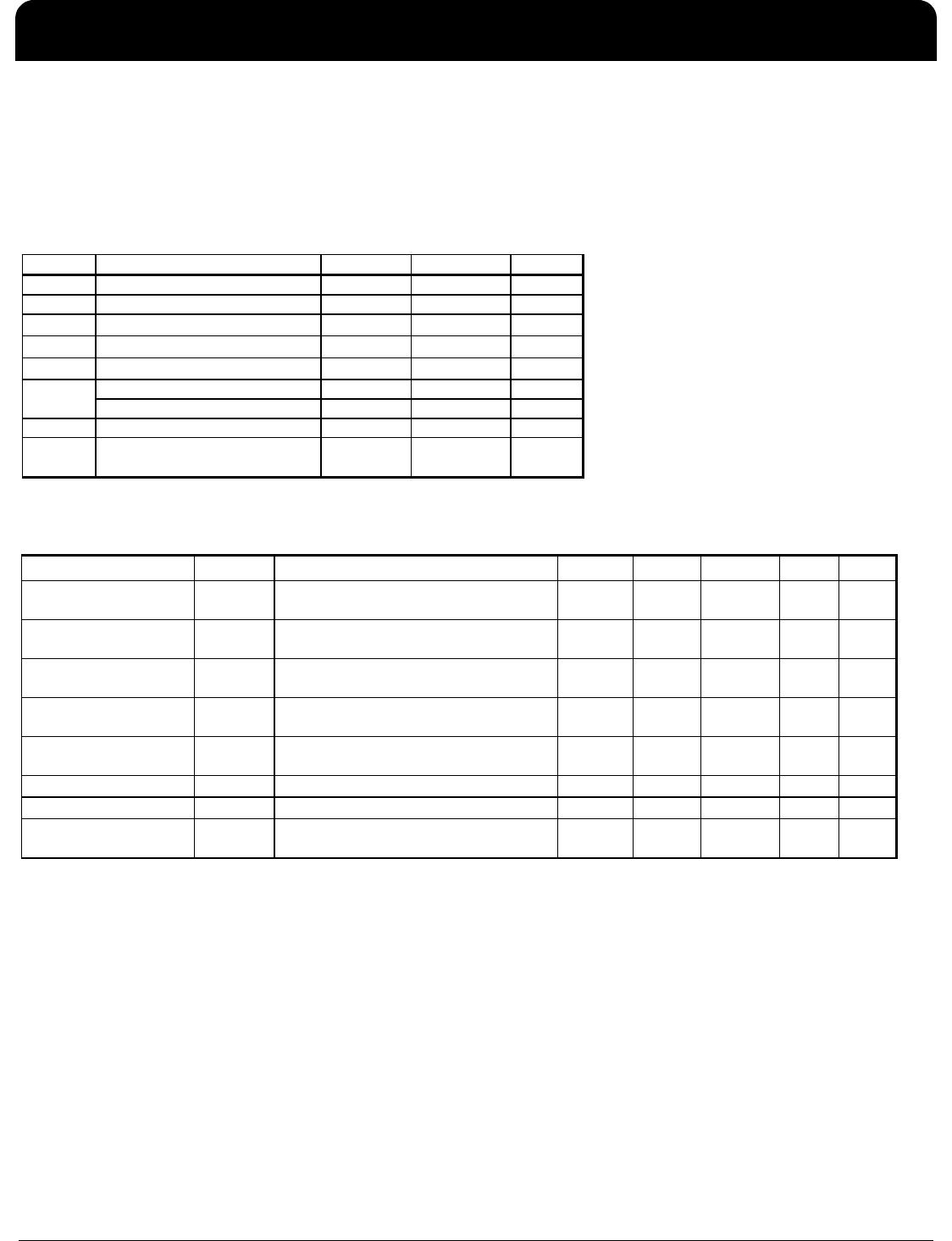
Electrical Characteristics–Input/Supply/Common Output Parameters
T
A
= Tambient for the desired operating range, Supply Voltage V
DD
= 3.3 V +/-5%
PARAMETER SYMBOL CONDITIONS MIN TYP MAX UNITS NOTES
Input High Voltage V
IHSE
2V
DD
+ 0.3 V 1
Input Low Voltage V
ILSE
GND - 0.3 0.8 V 1
Input High Current I
IHSE
V
IN
= V
DD
-5 5 uA 1
I
IL1
V
IN
= 0 V; Inputs with no pull-up resistors -5 uA 1
I
IL2
V
IN
= 0 V; Inputs with pull-up resistors -200 uA 1
I
DD3.3OPC
Full Active, C
L
= Full load; Commerical
Tem
p
Ran
g
e
175 200 mA 1
I
DD3.3OPI
Full Active, C
L
= Full load; Industrial
Tem
p
Ran
g
e
190 225 mA 1
all diff pairs driven, C-Temp 50 60 mA 1
all differential pairs tri-stated, C-Temp 4 6 mA 1
all diff pairs driven, I-temp 55 65 mA 1
all differential pairs tri-stated, I-temp 6 8 mA 1
I
DD3.3OPC
Full Active, C
L
= Full load; Commerical
Tem
p
Ran
g
e
105 125 mA 1
I
DD3.3OPI
Full Active, C
L
= Full load; Industrial
Tem
p
Ran
g
e
115 150 mA 1
all diff pairs driven, C-Temp 25 30 mA 1
all differential pairs tri-stated, C-Temp 2 3 mA 1
all diff pairs driven, I-Temp 30 35 mA 1
all differential pairs tri-stated, I-Temp 3 4 mA 1
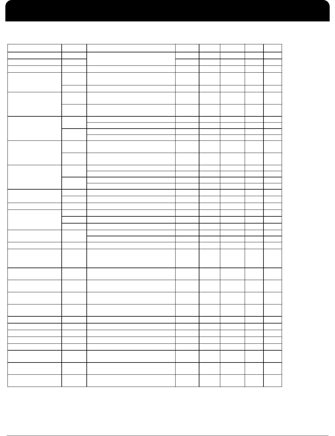
F
iPLL
PCIe Mode (Bypass#/PLL= 1) 50 100 MHz 1
F
iBYPASS
Bypass Mode ((Bypass#/PLL= 0) 33 400 MHz 1
Pin Inductance L
p
in
7nH1
C
IN
Logic Inputs, except SRC_IN 1.5 5 pF 1
C
INSRC_IN
SRC_IN differential clock inputs 1.5 2.7 pF 1,4
C
OUT
Output pin capacitance 6 pF 1
-3dB point in High BW Mode 2 3 4 MHz 1
-3dB point in Low BW Mode 0.7 1 1.4 MHz 1
PLL Jitter Peaking t
JPEAK
Peak Pass band Gain 1.5 2 dB 1
Clk Stabilization T
STAB
From V
DD
Power-Up and after input clock
stabilization or de-assertion of PD# to 1st
clock
1ms1,2
Input SS Modulation
Frequency
f
MODIN
Allowable Frequency
(Triangular Modulation)
30 33 kHz 1
OE# Latency t
LATOE#
DIF start after OE# assertion
DIF stop after OE# deassertion
1 3 cycles 1,3
Tdrive_SRC_STOP# t
DRVSTP
DIF output enable after
SRC_Stop# de-assertion
10 ns 1,3
Tdrive_PD# t
DRVPD
DIF output enable after
PD# de-assertion
300 us 1,3
Tfall t
F
Fall time of PD# and SRC_STOP# 5 ns 1
Trise t
R
Rise time of PD# and SRC_STOP# 5 ns 2
SMBus Voltage V
MAX
Maximum input voltage 5.5 V 1
Low-level Output Voltage V
OL
@ I
PULLUP
0.4 V 1
Current sinking at V
OL
I
PULLUP
4mA1
SCLK/SDATA
Clock/Data Rise Time
t
RSMB
(Max VIL - 0.15) to
(Min VIH + 0.15)
1000 ns 1
SCLK/SDATA
Clock/Data Fall Time
t
FSMB
(Min VIH + 0.15) to
(Max VIL - 0.15)
300 ns 1
SMBus Operating
Frequency
f
MAXSMB
Maximum SMBus operating frequency 100 kHz 1,5
1
Guaranteed by design and characterization, not 100% tested in production.
2
See timing diagrams for timing requirements.
I
DD3.3PDI
I
DD3.3PDI
9DB803 Powerdown
Current
Single Ended Inputs, 3.3 V +/-5%
Input Low Current
I
DD3.3PDC
9DB803 Supply Current
9DB403 Supply Current
9DB403 Powerdown
Current
5
The differential input clock must be running for the SMBus to be active
Input Frequency
4
SRC_IN input
I
DD3.3PDC
3
Time from deassertion until outputs are >200 mV
PLL Bandwidth BW
Capacitance
ICS9DB803D
EIGHT OUTPUT DIFFERENTIAL BUFFER FOR PCIE GEN1 AND GEN2
IDT®
EIGHT OUTPUT DIFFERENTIAL BUFFER FOR PCIE GEN1 AND GEN2 9
ICS9DB803D REV N 071013
Electrical Characteristics–DIF 0.7V Current Mode Differential Pair
T
A
=Tambient; V
DD
= 3.3 V +/-5%; C
L
=2pF, R
S
=33
, R
P
=49.9
, R
REF
=475
PARAMETER SYMBOL CONDITIONS MIN TYP MAX UNITS NOTES
Current Source Output
Impedance
Zo
1
3000
1
Voltage High VHigh 660 850 1,2
Voltage Low VLow -150 150 1,2
Max Voltage Vovs 1150 1
Min Voltage Vuds -300 1
Crossing Voltage (abs) Vcross(abs) 250 550 mV 1
Crossing Voltage (var) d-Vcross
Variation of crossing over all
edges
140 mV 1
Rise Time t
r
V
OL
= 0.175V, V
OH
= 0.525V 175 700 ps 1
Fall Time t
f
V
OH
= 0.525V V
OL
= 0.175V 175 700 ps 1
Rise Time Variation d-t
r
125 ps 1
Fall Time Variation d-t
f
125 ps 1
Duty Cycle d
t3
Measurement from differential
wavefrom
45 55 % 1
t
p
dBYP
Bypass Mode, V
T
= 50% 2500 4500 ps 1
t
p
dPLL
PLL Mode V
T
= 50% -250 250 ps 1
Skew, Output to Output t
sk3
V
T
= 50% 50 ps 1
PLL mode 50 ps 1,3
Additiv
e
Jitter in Bypass Mode 50 ps 1,3
PCIe Gen1 phase jitter
(Additive in Bypass Mode)
710
ps
(pk2pk)
1,4,5
PCIe Gen 2 Low Band phase jitter
(Additive in Bypass Mode)
00.1
ps
(rms)
1,4,5
PCIe Gen 2 High Band phase jitter
(Additive in Bypass Mode)
0.3 0.5
ps
(rms)
1,4,5
PCIe Gen 1 phase jitter 40 86
ps
(pk2pk)
1,4,5
PCIe Gen 2 Low Band phase jitter 1.5 3
ps
(rms)
1,4,5
PCIe Gen 2 High Band phase jitter
2.7/
2.2
3.1
ps
(rms)
1,4,5,6
1
Guaranteed by design and characterization, not 100% tested in production.
2
I
RE
F
= V
DD
/(3xR
R
). For R
R
= 475
(1%), I
RE
F
= 2.32mA. I
OH
= 6 x I
RE
F
and V
OH
= 0.7V @ Z
O
=50
.
3 Measured from differential waveform
4
See http://www.pcisig.com for complete specs
5
Device driven by 932S421C or equivalent.
6
First number is High Bandwidth Mode, second number is Low Bandwidth Mode
Statistical measurement on single
ended signal using oscilloscope
math function.
mV
Measurement on single ended
signal using absolute value.
mV
t
jphaseBYP
Jitter, Phase
t
jphasePLL
Skew, Input to Output
Jitter, Cycle to cycle t
jcyc-cyc

9DB803DFLF

Mfr. #:
Manufacturer:
IDT
Description:
Clock Buffer 8 OUTPUT PCIE GEN2 BUFFER
Lifecycle:
New from this manufacturer.
Delivery:
DHL FedEx Ups TNT EMS
Payment:
T/T Paypal Visa MoneyGram Western Union