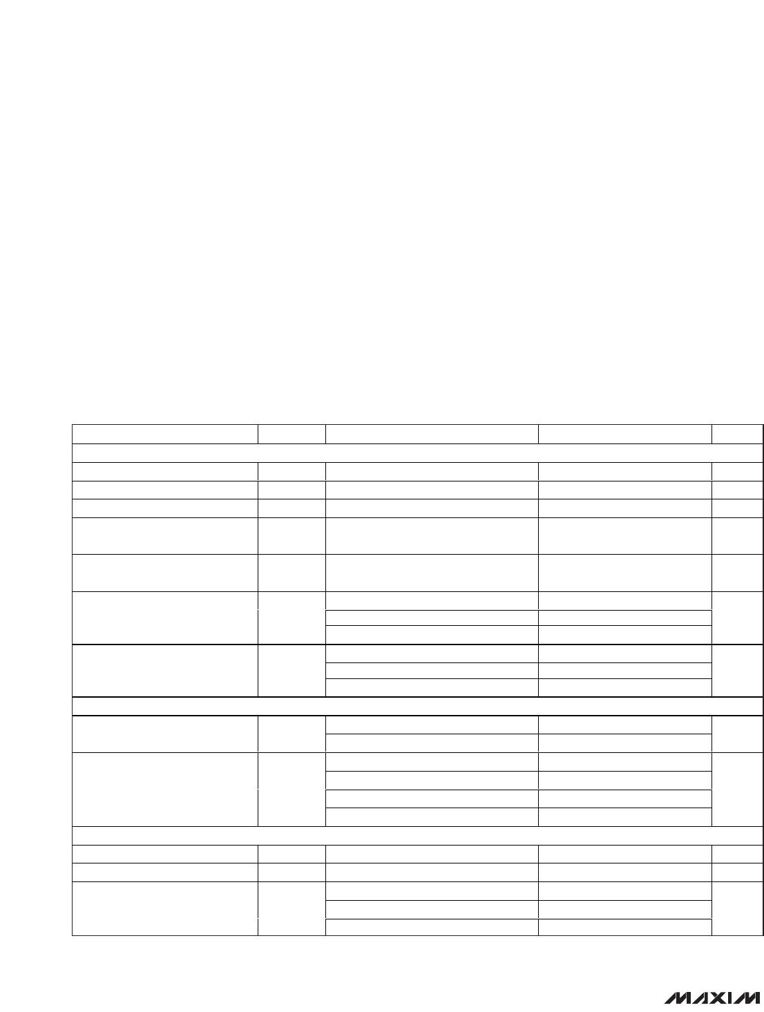
General Description
The MAX5417/MAX5418/MAX5419 nonvolatile, linear-
taper, digital potentiometers perform the function of a
mechanical potentiometer by replacing the mechanics
with a simple 2-wire digital interface, allowing communi-
cation with multiple devices. Each device performs the
same function as a discrete potentiometer or variable
resistor and has 256 tap points.
The devices feature an internal, nonvolatile EEPROM
used to store the wiper position for initialization during
power-up. The fast-mode I
2
C-compatible serial interface
allows communication at data rates up to 400kbps, mini-
mizing board space and reducing interconnection com-
plexity in many applications. Each device is available with
one of four factory-preset addresses (see the
Ordering
Information/Selector Guide
) and features an address
input for a total of eight unique address combinations.
The MAX5417/MAX5418/MAX5419 provide three nomi-
nal resistance values: 50k (MAX5417), 100k
(MAX5418), or 200k (MAX5419). The nominal resistor
temperature coefficient is 35ppm/°C end-to-end, and
only 5ppm/°C ratiometric. This makes the devices ideal
for applications requiring a low-temperature-coefficient
variable resistor, such as low-drift, programmable gain-
amplifier circuit configurations.
The MAX5417/MAX5418/MAX5419 are available in a
3mm x 3mm 8-pin TDFN package, and are specified
over the extended -40°C to +85°C temperature range.
Applications
Mechanical Potentiometer Replacement
Low-Drift Programmable-Gain Amplifiers
Volume Control
Liquid-Crystal Display (LCD) Contrast Control
Features
o Power-On Recall of Wiper Position from
Nonvolatile Memory
o Tiny 3mm x 3mm 8-Pin TDFN Package
o 35ppm/°C End-to-End Resistance Temperature
Coefficient
o 5ppm/°C Ratiometric Temperature Coefficient
o 50k/100k/200k Resistor Values
o Fast I
2
C-Compatible Serial Interface
o 500nA (typ) Static Supply Current
o Single-Supply Operation: +2.7V to +5.25V
o 256 Tap Positions
o ±0.5 LSB DNL in Voltage-Divider Mode
o ±0.5 LSB INL in Voltage-Divider Mode
MAX5417/MAX5418/MAX5419
256-Tap, Nonvolatile, I
2
C-Interface,
Digital Potentiometers
________________________________________________________________
Maxim Integrated Products
1
V
DD
GND
SDA
SCL
8-BIT
SHIFT
REGISTER
8-BIT
LATCH
8-BIT
NV
MEMORY
I
2
C
INTERFACE
A
0
8
8
256
W
L
256-
POSITION
DECODER
H
POR
MAX5417
MAX5418
MAX5419
Ordering Information/Selector Guide
Functional Diagram
19-3185; Rev 4; 4/10
For pricing, delivery, and ordering information, please contact Maxim Direct at 1-888-629-4642,
or visit Maxim’s website at www.maxim-ic.com.
Pin Configuration appears at end of data sheet.
+
Denotes a lead(Pb)-free/RoHS-compliant package.
**
Exposed pad.
PART TEMP RANGE I
2
C ADDRESS R (k) PIN-PACKAGE TOP MARK
MAX5417LETA+ -40°C to +85°C 010100A
0
50 8 TDFN-EP** AIB
MAX5417META+ -40°C to +85°C 010101A
0
50 8 TDFN-EP** ALS
MAX5417NETA+ -40°C to +85°C 010110A
0
50 8 TDFN-EP** ALT
MAX5417PETA+ -40°C to +85°C 010111A
0
50 8 TDFN-EP** ALU
MAX5418LETA+ -40°C to +85°C 010100A
0
100 8 TDFN-EP** AIC
MAX5418META+ -40°C to +85°C 010101A
0
100 8 TDFN-EP** ALV
MAX5418NETA+ -40°C to +85°C 010110A
0
100 8 TDFN-EP** ALW
MAX5418PETA+ -40°C to +85°C 010111A
0
100 8 TDFN-EP** ALX
MAX5419LETA+ -40°C to +85°C 010100A
0
200 8 TDFN-EP** AID
MAX5419META+ -40°C to +85°C 010101A
0
200 8 TDFN-EP** ALY
MAX5419NETA+ -40°C to +85°C 010110A
0
200 8 TDFN-EP** ALZ
MAX5419PETA+ -40°C to +85°C 010111A
0
200 8 TDFN-EP** AMA
MAX5417/MAX5418/MAX5419
256-Tap, Nonvolatile, I
2
C-Interface,
Digital Potentiometers
2 _______________________________________________________________________________________
ABSOLUTE MAXIMUM RATINGS
ELECTRICAL CHARACTERISTICS
(V
DD
= +2.7V to +5.25V, H = V
DD
, L = GND, T
A
= -40°C to +85°C, unless otherwise noted. Typical values are at V
DD
= +5V, T
A
= +25°C.)
Stresses beyond those listed under “Absolute Maximum Ratings” may cause permanent damage to the device. These are stress ratings only, and functional
operation of the device at these or any other conditions beyond those indicated in the operational sections of the specifications is not implied. Exposure to
absolute maximum rating conditions for extended periods may affect device reliability.
V
DD
to GND...........................................................-0.3V to +6.0V
All Other Pins to GND.................................-0.3V to (V
DD
+ 0.3V)
Maximum Continuous Current into H, L, and W
MAX5417......................................................................±1.3mA
MAX5418......................................................................±0.6mA
MAX5419......................................................................±0.3mA
Continuous Power Dissipation (T
A
= +70°C)
8-Pin TDFN (derate 24.4mW/°C above +70°C) .........1951mW
Operating Temperature Range ...........................-40°C to +85°C
Junction Temperature......................................................+150°C
Storage Temperature Range .............................-60°C to +150°C
Lead Temperature (soldering, 10s) .................................+300°C
Soldering Temperature (reflow) .......................................+260°C
PARAMETER SYMBOL CONDITIONS MIN TYP MAX UNITS
DC PERFORMANCE (VOLTAGE-DIVIDER MODE)
Resolution 256 Taps
Integral Nonlinearity INL (Note 1) ±0.5 LSB
Differential Nonlinearity DNL (Note 1) ±0.5 LSB
End-to-End Temperature
Coefficient
TC
R
35 ppm/°C
Ratiometric Temperature
Coefficient
5 ppm/°C
MAX5417_, 50 -0.6
MAX5418_, 100k -0.3Full-Scale Error
MAX5419_, 200k -0.15
LSB
MAX5417_, 50k 0.6
MAX5418_, 100k 0.3
Zero-Scale Error
MAX5419_, 200k 0.15
LSB
DC PERFORMANCE (VARIABLE-RESISTOR MODE)
V
DD
= 3V ±3
Integral Nonlinearity
(Note 2)
INL
V
DD
= 5V ±1.5
LSB
V
DD
= 3V, MAX5417_, 50k -1 +2
V
DD
= 3V, MAX5418_, 100k ±1
V
DD
= 3V, MAX5419_, 200k ±1
Differential Nonlinearity
(Note 2)
DNL
V
DD
= 5V ±1
LSB
DC PERFORMANCE (RESISTOR CHARACTERISTICS)
Wiper Resistance R
W
V
DD
= 3V to 5.25V (Note 3) 325 675
Wiper Capacitance C
W
10 pF
MAX5417_ 37.5 50 62.5
MAX5418_ 75 100 125
End-to-End Resistance R
HL
MAX5419_ 150 200 250
k
MAX5417/MAX5418/MAX5419
256-Tap, Nonvolatile, I
2
C-Interface,
Digital Potentiometers
_______________________________________________________________________________________ 3
ELECTRICAL CHARACTERISTICS (continued)
(V
DD
= +2.7V to +5.25V, H = V
DD
, L = GND, T
A
= -40°C to +85°C, unless otherwise noted. Typical values are at V
DD
= +5V, T
A
= +25°C.)
DIGITAL INPUTS
V
DD
= 3.4V to 5.25V 2.4
Input High Voltage (Note 4) V
IH
V
DD
< 3.4V 0.7 x V
DD
V
Input Low Voltage V
IL
V
DD
= 2.7V to 5.25V (Note 4) 0.8 V
Low-Level Output Voltage V
OL
3mA sink current 0.4 V
Input Leakage Current I
LEAK
±1 µA
Input Capacitance 5pF
DYNAMIC CHARACTERISTICS
MAX5417_ 100
MAX5418_ 50
Wiper -3dB Bandwidth (Note 5)
MAX5419_ 25
kHz
NONVOLATILE MEMORY
Data Retention T
A
= +85°C 50 Years
T
A
= +25°C 200,000
Endurance
T
A
= +85°C 50,000
Stores
POWER SUPPLY
Power-Supply Voltage V
DD
2.70 5.25 V
Standby Current I
DD
Digital inputs = V
DD
or GND,
T
A
= +25°C
0.5 1 µA
Programming Current
During nonvolatile write;
digital inputs = V
DD
or GND (Note 6)
200 400 µA
PARAMETER SYMBOL CONDITIONS MIN TYP MAX UNITS
ANALOG SECTION
MAX5417_ 500
MAX5418_ 600Wiper Settling Time (Note 8) t
IL
MAX5419_ 1000
ns
DIGITAL SECTION
SCL Clock Frequency f
SCL
400 kHz
Setup Time for START Condition t
SU-STA
0.6 µs
Hold Time for START Condition t
HD-STA
0.6 µs
CLK High Time t
HIGH
0.6 µs
CLK Low Time t
LOW
1.3 µs
TIMING CHARACTERISTICS
(V
DD
= +2.7V to +5.25V, H = V
DD
, L = GND, T
A
= -40°C to +85°C, unless otherwise noted. Typical values are at V
DD
= +5V, T
A
=
+25°C. See Figures 1 and 2.) (Note 7)

MAX5419LETA+T

Mfr. #:
Manufacturer:
Maxim Integrated
Description:
Digital Potentiometer ICs 256-Tap Nonvolatile I2C-Interface
Lifecycle:
New from this manufacturer.
Delivery:
DHL FedEx Ups TNT EMS
Payment:
T/T Paypal Visa MoneyGram Western Union