MAX5417/MAX5418/MAX5419
256-Tap, Nonvolatile, I
2
C-Interface,
Digital Potentiometers
_______________________________________________________________________________________
7
-0.2
-0.1
0
0.1
0.2
0.3
-0.3
DNL vs. TAP POSITION
(MAX5419)
MAX5417 toc15
TAP POSITION
DNL (LSB)
22419232 64 96 128 1600 256
VARIABLE-RESISTOR MODE
V
DD
= 2.7V
I
SRC
= 10
µ
A
MIDSCALE WIPER RESPONSE vs. FREQUENCY
(MAX5417)
MAX5417 toc16
FREQUENCY (kHz)
WIPER RESPONSE (dB)
10010
-25
-20
-10
-15
-5
MAX5417
TAP = 128
C
L
= 50pF
C
L
= 10pF
0
-30
1 1000
MIDSCALE WIPER RESPONSE vs. FREQUENCY
(MAX5418)
MAX5417 toc17
FREQUENCY (kHz)
WIPER RESPONSE (dB)
10010
-25
-20
-10
-15
-5
MAX5418
TAP = 128
C
L
= 50pF
C
L
= 10pF
0
-30
11000
MIDSCALE WIPER RESPONSE vs. FREQUENCY
(MAX5419)
MAX5417 toc18
FREQUENCY (kHz)
WIPER RESPONSE (dB)
10010
-40
-35
-30
-25
-20
-15
-10
-5
0
-45
1 1000
MAX5419
TAP = 128
C
L
= 10pF
C
L
= 50pF
TAP-TO-TAP SWITCHING TRANSIENT
(MAX5417)
MAX5417 toc19
W
10mV/div
SDA
2V/div
1
µ
s/div
MAX5417
C
L
= 10pF
FROM TAP 127
TO TAP 128
H = V
DD
TAP-TO-TAP SWITCHING TRANSIENT
(MAX5418)
MAX5417 toc20
W
10mV/div
SDA
2V/div
1µs/div
MAX5418
C
L
= 10pF
FROM TAP 127
TO TAP 128
H = V
DD
TAP-TO-TAP SWITCHING TRANSIENT
(MAX5419)
MAX5417 toc21
W
10mV/div
SDA
2V/div
1µs/div
MAX5419
C
L
= 10pF
FROM TAP 127
TO TAP 128
H = V
DD
Typical Operating Characteristics (continued)
(V
DD
= +5V, T
A
= +25°C, unless otherwise noted.)
MAX5417/MAX5418/MAX5419
256-Tap, Nonvolatile, I
2
C-Interface,
Digital Potentiometers
8 _______________________________________________________________________________________
Pin Description
PIN NAME FUNCTION
1V
DD
Power-Supply Input. 2.7V to 5.25V voltage range. Bypass with a 0.1µF capacitor from V
DD
to GND.
2 SCL I
2
C-Interface Clock Input
3 SDA I
2
C-Interface Data Input
4A
0
Address Input. Sets the A0 bit in the device ID address.
5 GND Ground
6 L Low Terminal
7 W Wiper Terminal
8 H High Terminal
—EP
Exposed Pad. Internally connected to GND. Connect to a large ground plane to maximize thermal
performance. Not intended as an electrical point.
t
HD-STA
t
SU-DAT
t
HIGH
t
R
t
F
t
HD-DAT
t
HD-STA
S Sr A
t
SU-STA
t
LOW
t
BUF
t
SU-STO
PS
t
R
t
F
SCL
SDA
PARAMETERS ARE MEASURED FROM 30% TO 70%.
Detailed Description
The MAX5417/MAX5418/MAX5419 contain a resistor
array with 255 resistive elements. The MAX5417 has a
total end-to-end resistance of 50k, the MAX5418 has
an end-to-end resistance of 100k, and the MAX5419
has an end-to-end resistance of 200k. The
MAX5417/MAX5418/MAX5419 allow access to the high,
low, and wiper terminals for a standard voltage-divider
configuration. H, L, and W can be connected in any
desired configuration as long as their voltages fall
between GND and V
DD
.
A simple 2-wire I
2
C-compatible serial interface moves
the wiper among the 256 tap points. A nonvolatile mem-
ory stores the wiper position and recalls the stored wiper
position in the nonvolatile memory upon power-up. The
nonvolatile memory is guaranteed for 50 years for wiper
data retention and up to 200,000 wiper store cycles.
Figure 1. I
2
C Serial-Interface Timing Diagram
V
DD
I
OL
= 3mA
I
OH
= 0mA
V
OUT
400pF
SDA
Figure 2. Load Circuit
MAX5417/MAX5418/MAX5419
256-Tap, Nonvolatile, I
2
C-Interface,
Digital Potentiometers
_______________________________________________________________________________________ 9
Analog Circuitry
The MAX5417/MAX5418/MAX5419 consist of a resistor
array with 255 resistive elements; 256 tap points are
accessible to the wiper, W, along the resistor string
between H and L. The wiper tap point is selected by
programming the potentiometer through the 2-wire (I
2
C)
interface. Eight data bits, an address byte, and a con-
trol byte program the wiper position. The H and L termi-
nals of the MAX5417/MAX5418/MAX5419 are similar to
the two end terminals of a mechanical potentiometer.
The MAX5417/MAX5418/MAX5419 feature power-on
reset circuitry that loads the wiper position from non-
volatile memory at power-up.
Digital Interface
The MAX5417/MAX5418/MAX5419 feature an internal,
nonvolatile EEPROM that stores the wiper state for ini-
tialization during power-up. The shift register decodes
the control and address bits, routing the data to the
proper memory registers. Data can be written to a
volatile memory register, immediately updating the
wiper position, or data can be written to a nonvolatile
register for storage.
The volatile register retains data as long as the device
is powered. Once power is removed, the volatile regis-
ter is cleared. The nonvolatile register retains data even
after power is removed. Upon power-up, the power-on
reset circuitry controls the transfer of data from the non-
volatile register to the volatile register.
Serial Addressing
The MAX5417/MAX5418/MAX5419 operate as a slave
that receives data through an I
2
C- and SMBus™-com-
patible 2-wire interface. The interface uses a serial data
access (SDA) line and a serial clock line (SCL) to
achieve communication between master(s) and
slave(s). A master, typically a microcontroller, initiates
all data transfers to the MAX5417/MAX5418/MAX5419,
and generates the SCL clock that synchronizes the
data transfer (Figure 1).
The MAX5417/MAX5418/MAX5419 SDA line operates
as both an input and an open-drain output. A pullup
resistor, typically 4.7k, is required on the SDA bus.
The MAX5417/MAX5418/MAX5419 SCL operates only
as an input. A pullup resistor, typically 4.7k, is
required on the SCL bus if there are multiple masters
on the 2-wire interface, or if the master in a single-mas-
ter system has an open-drain SCL output.
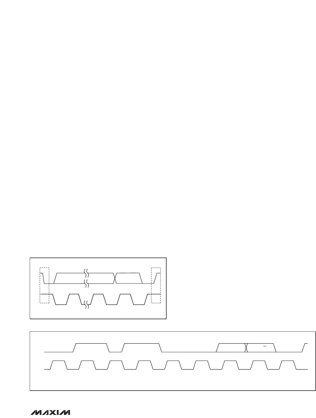
Each transmission consists of a START (S) condition
(Figure 3) sent by a master, followed by the
MAX5417/MAX5418/MAX5419 7-bit slave address plus
the 8th bit (Figure 4), 1 command byte (Figure 7) and 1
data byte, and finally a STOP (P) condition (Figure 3).
Start and Stop Conditions
Both SCL and SDA remain high when the interface is
not busy. A master signals the beginning of a transmis-
sion with a START condition by transitioning SDA from
high to low while SCL is high. When the master has fin-
ished communicating with the slave, it issues a STOP
condition by transitioning the SDA from low to high
while SCL is high. The bus is then free for another
transmission (Figure 3).
Bit Transfer
One data bit is transferred during each clock pulse.
The data on the SDA line must remain stable while SCL
is high (Figure 5).
SDA
START
CONDITION
SCL
S
STOP
CONDITION
P
Figure 3. Start and Stop Conditions
SDA
SCL
*See the Ordering Information/Selector Guide section for other address options.
01
A0
MSB LSB
NOP/W ACK
0 1 0* 0*
Figure 4. Slave Address
SMBus is a trademark of Intel Corporation.

MAX5419LETA+T

Mfr. #:
Manufacturer:
Maxim Integrated
Description:
Digital Potentiometer ICs 256-Tap Nonvolatile I2C-Interface
Lifecycle:
New from this manufacturer.
Delivery:
DHL FedEx Ups TNT EMS
Payment:
T/T Paypal Visa MoneyGram Western Union