LT3092
13
3092fc
For more information www.linear.com/LT3092
applicaTions inForMaTion
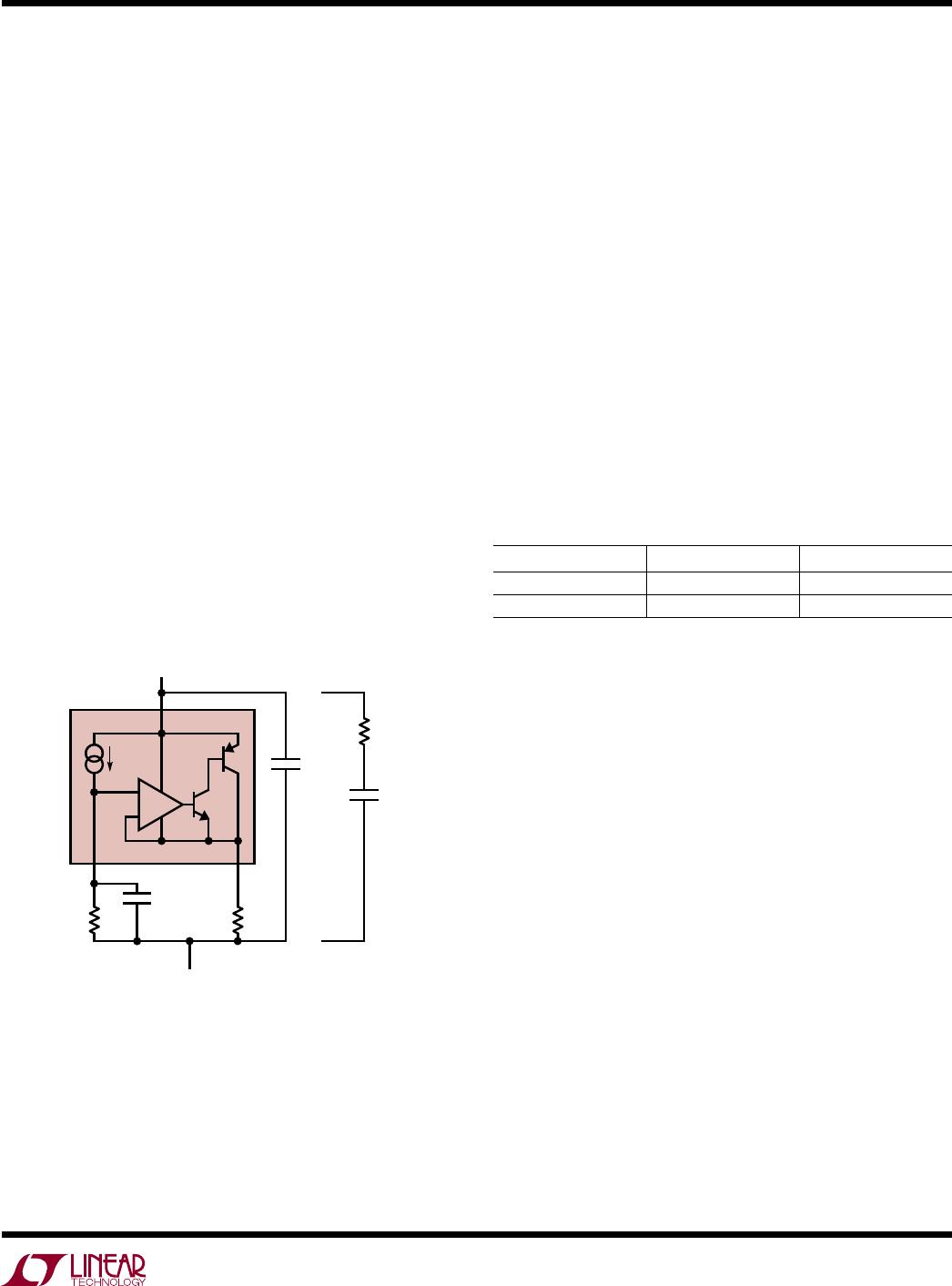
Quieting the Noise
When a reduction in the noise of the current source is
desired, a small capacitor can be placed across R
SET
(C
SET
in Figure 7). Normally, the 10µA reference current source
generates noise current levels of 2.7pA/√Hz (0.7nA
RMS
over the 10Hz to 100kHz bandwidth). The SET pin resistor
generates a spot noise equal to i
n
= √4kT/R (k = Boltzmann’s
constant, 1.38 • 10
–23
J/°K, and T is absolute temperature)
which is RMS-summed with the noise generated by the
10µA reference current source. Placing a C
SET
capacitor
across R
SET
(as shown in Figure 7) bypasses this noise
current. Note that this noise reduction capacitor increases
start-up time as a factor of the time constant formed by
R
SET
• C
SET
. When using a capacitor across the SET pin
resistor, the external pole introduced usually requires
compensation to maintain stability. See the Stability and
Frequency Compensation section for detailed descriptions
on compensating LT3092 circuits.
A curve in the Typical Performance Characteristics section
depicts noise spectral density for the reference current
over a 10Hz to 100kHz bandwidth.
Paralleling Devices
Obtain higher output current by paralleling multiple
LT3092’s together. The simplest application is to run
two current sources side by side and tie their inputs
together and their outputs together, as shown in Figure
8. This allows the sum of the current sources to deliver
more output current than a single device is capable of
delivering.
Another method of paralleling devices requires fewer
components and helps to share power between devices.
Tie the individual SET pins together and tie the individual
IN pins together. Connect the outputs in common using
small pieces of PC trace as ballast resistors to promote
equal current sharing. PC trace resistance in milliohms/
inch is shown in Table 1. Ballasting requires only a tiny
area on the PCB.
Table 1. PC Board Trace Resistance
WEIGHT (oz) 10mil WIDTH 20mil WIDTH
1 54.3 27.1
2 27.1 13.6
Trace resistance is measured in mΩ/in
The worst-case room temperature offset, only ±2mV be-
tween the SET pin and the OUT pin, allows the use of very
small ballast resistors.
As shown in Figure 9, each LT3092 has a small 40mΩ
ballast resistor, which at full output current gives better
than 80% equalized sharing of the current. The external
resistance of 40mΩ (20mΩ for the two devices in paral
-
lel) only adds about 8mV of output voltage compliance at
an output of 0.4A
. Of course, paralleling more than two
LT3092’s yields even higher output current. Spreading the
device on the PC board also spreads the heat. Series input
resistors can further spread the heat if the input-to-output
difference is high.
Thermal Considerations
The LT3092’s internal power and thermal limiting circuitry
protects itself under overload conditions. For continuous
normal load conditions, do not exceed the 125°C maximum
junction temperature. Carefully consider all sources of
thermal resistance from junction-to-ambient. This includes
(but is not limited to) junction-to-case, case-to-heat sink
Figure 7. Adding C
SET
Lowers Current Noise
3092 F07
IN
SET OUT
+
–
LT3092
10µA
C
COMP
OR
R
SET
R
OUT
R
COMP
C
COMP
C
SET

